Unit Description
(Notice: This version of Unit Description describes the NVDLA design as it exists in the nvdlav1 release. The other releases and configurations are similar but won’t contain all features and sizes of hardware elements may differ.)
Please refer to Scalability parameters and ConfigROM for other configurations.)
Bridge DMA
Overview
Input images and processed results are stored in external DRAM, but external DRAM bandwidth and latency are generally insufficient to allow NVDLA to fully utilize it’s MAC arrays. Therefore NVDLA is configured with a secondary memory interface to on-chip SRAM.
To utilize the on-chip SRAM, NVDLA needs to move data between external DRAM and SRAM. Bridge DMA is proposed to full-fill this purpose. There are two independent paths, one is copies data from external DRAM to internal SRAM , and the other one is copies data from internal SRAM to external DRAM. Both directions cannot work simultaneously. BDMA can also move data from external DRAM to external DRAM, or from internal SRAM to internal SRAM.
Bridge DMA has two DMA interfaces, one connects to external DRAM, and the other connects to internal SRAM. Both two interfaces support read and write requests. The data widths of both interfaces are 512 bits, and the maximum burst length is 4.
In order to move all data in a cube, BDMA support line repeat which can fetch multiple lines with address jumps between lines, reflect a surface. And also, BDMA will support one more layer of repeat, that fetch of multiple lines can be repeated, which reflect multiple surfaces, reflect a cube.
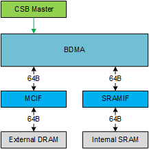
Fig. 37 Bridge DMA
Convolution Pipeline
Overview
The Convolution Pipeline is one of pipelines within the NVDLA core logic. It is used to accelerate the convolution algorithm. It supports comprehensive programmable parameters for variable convolution sizes. Some features like Winograd and multi-batch are applied within the convolution pipeline to improve the performance and increase MAC efficiency.
The Convolution Pipeline has five stages, which are: Convolution DMA, Convolution Buffer, Convolution Sequence Controller, Convolution MAC and Convolution Accumulator. They are also called CDMA, CBUF, CSC, CMAC and CACC respectively. Each stage has its own CSB slave port to receive configuration data from the controlling CPU. A single synchronization mechanism is used by all stages.
The Convolution Pipeline supports three types of operations. They are:
Direct convolution for feature data, or DC mode
Convolution of image input, or image input mode
Winograd convolution, or Winograd mode
The convolution pipeline contains 1024 MACs for int16 or fp16, along with a 32 element accumulator array for partial sum storage. The MAC resources can also be configured to provide 2048 MACs for int8. Additionally, there is 512KB of SRAM in convolution buffer, providing input weight and activation storage. These units are described in detail later in this document.
Below is the diagram of convolution pipeline.
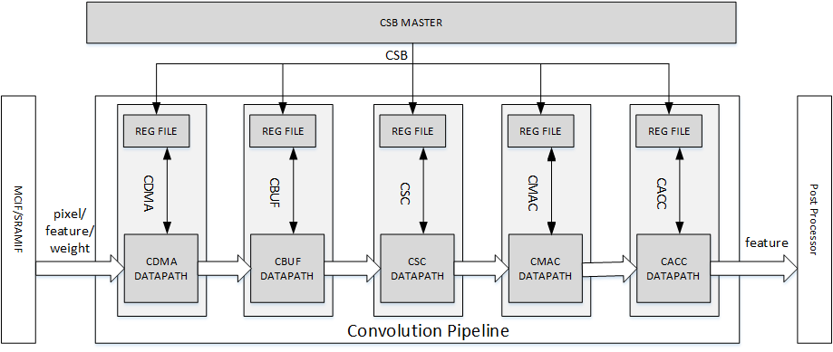
Fig. 38 Convolution Pipeline
Direct Convolution
The convolution pipeline always has two parts of input data. One is input activation data, the other is weight data. Suppose NVDLA engine has such input parameters:
Size of feature data cube: WxHxC
Size of one weight kernel: RxSxC
Total kernel number: K
Zero padding size: LP at left boundary, RP at right boundary, TP at top boundary, BP at bottom boundary.
Convolution stride: SX in X dimension, SY in Y dimension
Dilation: DX in X dimension, DY in Y dimension
Size of output data cube: W’xH’xC’
Fig. 39 Convolution operation
Figure below shows the convolution stride and zero padding.
Fig. 40 Convolution stride and zero padding
Then the equations of these parameters are:
The relationship of each element y in output data cube, element x in input feature data cube and element wt in weight kernels is:
The coordinate w,h,c,k in above equations are all start from zero.
To accomplish the convolution operation in the above equation, the convolution pipeline uses a method called direct convolution. The key idea of direct convolution is to split the multiplication oerations from each convolution kernel into groups such that each group contains 64 multiplications. The basic rules are:
Distribute all MACs hardware into 16 sub units. One sub unit is called MAC Cell, and has hardware for 64 int16/fp16 MACs, or for 128 int8 MACs.
The assembly of MAC Cells is called MAC Cell Array.
Divide all input data cubes into 1x1x64 element small cubes for int16, fp16 and int8.
Divide all weight data cubes into 1x1x64 element small cubes for int16, fp16 and int8.
Multiply one small input data cube by one small weight data cube, and add products together. These multiplications and additions are performed within one MAC cell.
Combine these compute operations into 4 operation levels, which are atomic operation, stripe operation, block operation and channel operation.
The four operations are described below using int6 percision mode as an example.
Atomic Operation
Atomic Operation is the base step for direct convolution. In one atomic operation, each MAC cell caches one 1x1x64 weight cubes from an individual weight kernel. The 16 MAC cells therefor cache weights from 16 int16/fp16 kernels or 32 int8 kernels. One 1x1x64 atomic cube of feature data is shared by all MAC cells. The MAC cells perform computing mentioned in rule 5 above. The output of each MAC cell is called a partial sum. This operation takes 1 cycle to complete, resulting in 16 partial sums per cycle. Partial sums are sent to the convolution accumulator module for further calculation.
The equation for the partial sum is:
In the equation, PS refers to partial sum. Variable c is always divisible by 64.
A diagram showing the Atomic Operation is as below.
Fig. 41 Atomic operation
Stripe Operation
A stripe operation combines a group of atomic operations from several convolutions. During one stripe operation the weight data in MAC cell array is kept unchanged. Input data slides along input data cube.
Notice the partial sums in one stripe operation cannot be added together as the correspond to different points in the output cube.
The length of stripe operation has limitations. The lower limit 16 is due to internal bandwidth to fetch weights for next stripe operation. The upper limit is 32 due to buffer size in the accumulator. The length may be less than lower limit in some extreme cases.
The figure below shows an example of stripe operation which contains 16 atomic operations. The padding size is 0 in this case. Notice it’s not a progressive scanning of input data cube. Though generally, a stripe does scan along the w dimension first. The figure below shows an example with no padding so the last two columns aren’t part of the first stripe (with a 3x3 kernel, no padding, and an input with w=6, the output will have a w of 4).
Fig. 42 Stripe operation
Block operation
A Block Operation is a higher level operation consisting of multiple stripe operations. During Block Operation, each kernel in a kernel group uses RxSx64 weight elements, along with a small cube of input feature data sized properly to ensure that the results can add together across stripe operations and accumulated into the 16-32 element accumulator.
Fig. 43 Block operation
All stripe operations in one block operation have the same atomic operation number. The partial sums from the same block operation are added together per stripe operation in the convolution accumulator. These results are called accumulative sum.
The equation of accumulative sum is:
In the equation, AS refers to accumulative sum. Variable c is always divisible by 64.
Channel Operation
Channel operation is an even higher-level operation. It includes (C+63)/64 block operations. The block operations in one channel operation are similar, except the coordinate of channel direction is different, showing as below
Fig. 44 Channel operation
All partial sums of one channel operation can be added together by stripe operation. After a channel operation, the result in convolution accumulator is exactly the convolution result.
The equation for the result of a channel operation s:
This equation is identically equal to the original convolution equation for a stripe of 16-32 output points. After one channel operation, the accumulator is unloaded and sent to the post-processor, making room for the next channel operation.
Group Operation
Group operation is a higher-level operation than channel operation. It includes about int((dataout_height * dataout_width) / stripe_size) channel operations. After a group operation, the output data composes a W x H x K’ output surface. Here K’ refers to kernel size in a kernel group, with one kernel group being the number of kernels processed at a time, one per MAC Cell.
Output Sequence
The sequence mentioned in each operation is mainly for input feature data and weight data, but not the output sequence. The output data sequence is quite simple. It follows the order of C’(K’)->W->H->C(K). Here C’ or K’ refers to kernel group size, which is 16 for int16/fp16 and 32 for int8.
The output order of direct convolution is consistent with feature memory mapping order.
Fig. 45 Output sequence of a partition
Operation for Int8 and fp16
The operations mentioned above reflect int16 precision. Fp16 is handled identically. However, int8 is handled a bit differently.
In convolution pipeline, each multiply-accumulate primitive for int16/fp16 is split into two MACs for int8. The element throughput of int8 is therefore double the int16 element throughput.
The table below records parameters of one atomic operation.
Convolution Precision |
Input Data Elements |
Weights per Kernel |
Kernels |
Output Elements |
|---|---|---|---|---|
int16 |
64 |
1024 |
16 |
16 |
fp16 |
64 |
1024 |
16 |
16 |
int8 |
64 |
2048 |
32 |
32 |
Winograd Convolution
Winograd convolution refers to an optional algorithm to optimize the performance of direct convolution. The Convolution Pipeline supports Winograd only for 3x3xC size kernels.
The motivation for the Winograd convolution is to reduce the number of multiplications required, resulting in drastically increased performance for a given number of MAC hardware elements.
Winograd requires some additional adders to perform the Winograd transform on input and output activation data.
The equation for the Winograd Convolution used in the Convolution Pipeline is:
Here symbol ⊙ indicates element-wise multiplication. Symbol g is a 3x3 kernel and d is a 4x4 tile of input data cube. Symbol S is the convolution result of g and d. It’s a 2x2 matrix.
A, G and C are matrices to transform the weight and input feature data.
Suppose \(U=GgG^{T}\) and \(V=C^{T}dC\), then the equation is:
According to the equation, the multiplication with A, G and C can be implemented with adders. Only 16 multiplications are required to calculate 4 results for a 3x3 kernel, while in direct convolution mode 36 multiplications are required. Winograd is therefore 2.25 times the performance of Direct Convolution.
Step \(U=GgG^{T}\) converts 3x3 kernel to 4x4 kernel used for a point-wise multiplication against a 4x4 patch of the input activation cube. Software should convert weight kernel before NVDLA engine is running. The Convolution Pipeline handles the conversion of input feature data and the result of multiplications.
Unlike in Direct Convolution, the Winograd Convolution Pipeline will divide kernels and input feature data into 4x4x4 element small data cubes. Before the MAC Cell, extra adders are used to convert these cubes with matrix \(C^{T}\) and C. This step is called PRA.
In one Winograd atomic operation, 64 products in one MAC cell are not simply added together as in Direct Convolution. The addition has three phases:
Phase 1, each of 4 products in the channel direction are added together. The output of phase 1 is 16 partial sums, representing a 4x4 matrix.
Phase 2, each 4x4 partial sum matrix is multiplied with matrix \(A^{T}\). The output of phase 2 is 8 partial sums, or a 4x2 matrix.
Phase 3, each 4x2 partial sum matrix from phase 2 is multiplied with matrix A. The output is 4 partial sums.
Then 4 partial sums are stored in accumulator for further calculation. Both phase 2 and phase 3 are called POA.
Winograd mode also has five operations. The comparing of parameters is listed in table below.
mode |
direct convolution |
direct convolution |
Winograd |
Winograd |
|---|---|---|---|---|
formats |
int16/fp16 |
int8 |
int16/fp16 |
int8 |
small data cube per MAC cell |
1x1x64 |
1x1x64 |
4x4x4 |
4x4x4 |
kernels per atomic operation |
16 |
32 |
16 |
32 |
atomics operation per stripe operation |
16~32 |
16~32 |
16~32 |
16~32 |
strips operation per block operation |
R*S |
R*S |
1 |
1 |
blocks operation per channel operation |
C/64 |
C/64 |
C/4 |
C/4 |
The output sequence of Winograd convolution is similar to direct convolution. Some differences of Winograd:
For Winograd operation, the output width and height shall be divisible by 4. It’s a mandatory requirement. It’s for special scan order.
The scan order of stripe operation in Winograd convolution is different from direct convolution. Please see figure below.
The block operation always has only one stripe operation.
Winograd layer always outputs 4 lines in parallel. SDP will guarantee the correction of memory mapping of output data cube.
Fig. 46 Scan order of stripe operation in Winograd (W-H projection)
Deconvolution
Deconvolution is a type of special convolution. It is some kind of inverse operation of normal convolution. Unlike normal convolution case, deconvolution layer always enlarges the data cube after calculation.
In the NVDLA architecture, deconvolution is a SW feature. From HW perspective, a SW deconvolution layer consists of a serial convolution layer and a contract layer supported by the RUBIK unit.
Fig. 47 is an example of a one-dimensional deconvolution layer. The Input data cube has dimensions W x 1 x 1 and kernel dimensions are 3 x 1 x 1. Though the calculation flow is different from convolution, the result formula is:
The formula is very similar to convolution formula, except weight R/S order is reversed. More generally, the formula of a WxHxC input data cube with K SxRxC kernels is:
According to equation, the 3D deconvolution is equal to a convolution with (S-1) and (R-1) zero padding and reversed R/S weight order
Fig. 47 One-dimensional deconvolution, x stride = 1
If the deconvolution X stride or Y stride is not 1, the calculation flow is a bit different. The weight kernels are split into smaller kernel sets. Each set of kernels operates as a convolution layer where X and Y strides are equal to 1. Several convolution layers are therefore used to generate a deconvolution layer result.
After a serial convolution layer, all deconvolution result values are ready but the mapping order is not expected result. If we append the convolutional output cube one after another in C direction, then the total output data cube is the Winograd channel-extended data cube. The extension parameter is deconv_x_stride and deconv_y_stride.
So, NVDLA uses a special layer contract layer (performed by Rubik) to reorder these output values to get the desired deconvolutional output cube.
In conclusion, NVDLA supports deconvolution layer by below strategy:
NVDLA use two steps to perform a deconvolution layer which stride is bigger than 1
The first step is a serial convolution layers with order-reversed kernels.
The output of first step forms a Winograd channel-extended output data cube. Extension parameter is deconvolution x stride and deconvolution y stride.
The second step is running on RUBIK units.
Rubik unit does an inverse operation to Winograd channel-extended data cube.
After the second HW-layer, the output data cube is formated as per the expected result.
Convolution with Image Input
NVDLA supports convolution with image data with a special mode to improve MAC utilization. Here image data could be a part or whole image surface. However, NVDLA can only support it for direct convolution. DC, Winograd and deconvolution layer cannot use pixel formats. Multi-batch option is also not supported for image input.
Comparing to DC, image input case has some difference:
Channel pre-extension. The weight kernel should do channel pre-extension. It is unlike DC mode or Winograd mode.
Data mapping in convolution buffer. The image data mapping in the convolution buffer is different from DC and Winograd mode. All elements of left and right padding and input pixel line are compactly residing in CBUF entries. See figure below. If channel size is 4, the element mapping order is R(Y)->G(U)->B(V)->A(X). If channel size is 3, the order is R(Y)->G(U)->B(V).
Distribution of stripe operation. The stripe operation length is fixed to 64. And stripe operation shall never across lines. So that every stripe operation is started from first byte of a CBUF entry.
Use channel post-extension for speedup. Even with channel pre-extension, usually kernel channel size is less than 32. Therefore, channel post-extension is very useful for image input convolution layer.
Fig. 48 Pixel mapping in convolution buffer
Channel Post-Extension
Channel post-extension is an option for improving MAC utilization for convolution with image input.
In the Convolution Pipeline, one atomic operation requires 64 elements in channel dimension (excluding Winograd mode). If the channel size of the input data cube is less than 64, MACs are not 100% utilized in each cycle. Thus, MAC efficiency depends on channel size in DC mode and image input mode.
The basic idea of channel post-extension is doing a vertical extension to enlarge the channel size during runtime.
For example, an image input layer has 4x4x4 kernel size. If post-extension is not enabled, the pre-extended channel size is 16 and efficiency of MACs drops to 25%. However, if post-extension parameter is set to 4, every atomic cycle convolution pipeline will fetch 4 neighboring lines and combine them as a C=64 line. Then MAC efficiency rise back to 100%.
Some limitation of channel post-extension:
Channel post-extension is only for image input convolution.
Channel post-extension only supports 2-line extending and 4-line extending.
Channel post-extension is limited by pre-extended channel size and convolution x stride
Channel post-extension |
conv_x_stride limit |
pre-extended channel size limit |
|---|---|---|
1-line |
No |
No |
2-lines |
(conv_x_stride * ori_channel_size) <=32 |
<=32 |
4-lines |
(conv_x_stride * ori_channel_size) <=16 |
<=16 |
It’s necessary to mention that the channel post-extension number (N) doesn’t need to be less than kernel height (R). Hardware can automatically tailor the redundant lines to avoid them be involved in computation. However, this also means the user shouldn’t expect N times of MAC efficiency improvements for this case.
Multi-Batch Mode
NVDLA engine also supports multi-batch to enhance the performance and reduce the bandwidth, especially for Fully-Connected (FC) layers. The output of one FC layer is a 1x1xC data cube. That means all weights in one FC layer are used only once. One stripe operation in FC layer has only one atomic operation. But the convolution pipeline needs 16 cycles to load weight for next atomic operation. This introduces a lot of bubbles in the pipeline and MAC efficiency falls to 6.25%. To save the efficiency, the NVDLA engine can apply multi-batch mode.
The multi-batch is a special option for DC mode with multiple input feature data cubes being processed at once. The Convolution pipeline will fetch multiple input data cubes for one set of weight kernels. This also changes the atomic operation. Small cubes from different input data cubes are loaded interlaced for atomic operation one after another. The stripe operation then contains atomic operations for multiple batches. Since weights are reused accross a stripe weight loading cycles are hidden and the efficiency increases.
The length of stripe operation with different batch size are:
Batch Size |
1 |
2 |
3 |
4 |
5 |
6 |
|---|---|---|---|---|---|---|
Normal length |
16 |
8x2 |
8x3 |
4x4 |
4x5 |
4x6 |
Max length |
32 |
16x2 |
16x3 |
8x4 |
8x5 |
8x6 |
Batch Size |
7 |
8 |
9 |
10 |
11 |
12 |
Normal length |
4x7 |
2x8 |
2x9 |
2x10 |
2x11 |
2x12 |
Max length |
8x7 |
4x8 |
4x9 |
4x10 |
4x11 |
4x12 |
Batch Size |
13 |
14 |
15 |
16~32 |
||
Normal length |
2x13 |
2x14 |
2x15 |
1xN |
||
Max length |
4x13 |
4x14 |
4x15 |
1xN |
Fig. 49 Multi-batch mode
Dilation
Dilation is an option that enlarges the kernel in R and S dimensions with zero values. This function can be enabled by SW according as needed.
The diagram below shows a case with the dilation parameter = 3.
Fig. 50 Weight dilation
NVDLA supports dilation in both R and S dimensions.
Limits of dilation:
Dilation is available for DC mode only.
Dilation is not available for Winograd or image input mode.
Power Consideration
Convolution pipeline supports clock gating for each major pipeline stage. If the pipeline stage is idle and no valid HW-layer is available, the data path of pipeline stage will be clock gated.
Convolution DMA
Overview
Convolution DMA (CDMA) is a pipeline stage in the convolution pipeline. It fetches data from SRAM/DRAM for the convolution operation and stores it into a buffer (Convolution Buffer or CBUF) in the order needed for the convolution engine. Supported input formats are:
Pixel data
Feature data
Uncompressed/compressed weight
WMB
WGS
Two read channels connect from CDMA to the AXI interface. These are the weight read channel, and data read channel. To fetch the input formats listed above, the channels are configured for that format formats. The table below records the input data format to read channel mapping.
Input Format |
Image Case |
Uncompressed Feature Case |
Uncompressed Weight Case |
Compressed Weight Case |
|---|---|---|---|---|
Pixel data |
data channel |
NA |
NA |
NA |
Uncompressed feature data |
NA |
data channel |
NA |
NA |
Uncompressed weight |
NA |
NA |
weight channel |
NA |
Sparse compressed weight |
NA |
NA |
NA |
weight channel |
WMB |
NA |
NA |
NA |
weight channel |
WGS |
NA |
NA |
NA |
weight channel |
Convolution DMA sends memory read requests only. All memory read requests sent by Convolution DMA are 64-byte aligned.
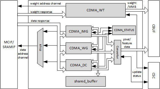
Fig. 51 Convolution DMA
CDMA consists of three sub-modules to fetch pixel data or feature data for convolution: CDMA_DC, CDMA_WG and CDMA_IMG. The procedures of these sub modules are similar, but differ in how they order the data into the CBUF RAM. At any time, only one of the sub modules is activated to fetch pixel/feature data.
Take CDMA_DC as an example to introduce the procedures:
Check status of convolution buffer for enough free space.
Generate read transactions
Cache feature data in shared buffers
Reshape feature cubes into proper order
Generate convolution buffer write address
Write feature data into convolution buffer
Update status of convolution buffer in the CDMA_STATUS sub-module
Convolution DMA uses a dedicated engine to handle the requirements of Winograd. CDMA_WG has very similar structure and functionality to CDMA_DC. However, the resulting feature data orginization in the convolution buffer is different. Thus CDMA_WG has a special fetching sequence. Additionally, CDMA_WG always performs Winograd channel extension.
The CDMA_IMG engine fetches pixel data from external memory. It generates the address according to the data format, reorders the pixel elements, and writes them into the proper entry of the convolution buffer. The basic behavior of CDMA_IMG is like CDMA_DC, but it operates on pixel data.
Only the CDMA_DC engine supports multi-batch mode. That is, fetching more than one input feature data cube in one HW-layer to improve the performance. The max batch size can be up to 32.
CDMA also use a dedicated engine for weight fetching: CDMA_WT. CDMA_WT is simple compared to other DMA engines, except that it can support three read steams at a time. If the input weight format is uncompressed, it only fetches weight data. If the input weight format is compressed, weight, WMB, and WGS are all fetched. Please see Data Formats for more details of weight formats.
If the input weight data is compressed, two arbiters are enabled for order of read streams. First a weighted round-robin arbiter grants a request from the weight stream or the WMB stream. Then the winner competes with the WGS request steam with a static priority arbitration. WGS always has priority. The final winning request is sent to weight channel for data fetching.
CDMA_WT always tries to fill the convolution buffer as much as possible, until the free entries runs out or weight fetching is complete.
CDMA maintains and communicates status of both the weight buffer and input data buffer in CBUF. There are two copies of status in CDMA and CSC. Two modules exchange the update/release information to decide when to fetch new feature/pixel/weight data and when to release these data elements.
Power Consideration
Convolution DMA applies clock gating in the data path. The clock of data path of convolution DMA is gated when it is idle and no hardware layer is configured in the programmable registers. The regfile sub module inside convolution DMA is not clock gated so that new commands can be programmed.
Convolution Buffer
Overview
The Convolution Buffer (CBUF) is a stage in convolution pipeline. It contains a total of 512KB of SRAM. The SRAMs cache input pixel data, input feature data, weight data and WMB data from CDMA module, and are read by convolution sequence generator module. CBUF has two write ports and three read ports.
CBUF contains of 16 32KB banks. Each bank consists of two 512-bit-wide, 256-entry two-port SRAMs. These banks act as three logical circular buffers:
Input data buffer
Weight buffer
WMB buffer
If the weight format is compressed, bank15 is assigned for WMB buffer, while two other buffers can use bank0~bank14. If weight format is uncompressed, WMB buffer is not assigned with any bank. In this case data buffer and weight buffer can fully use all 16 banks. If total required banks are less than 16, the remaining banks are unused.
Each buffer acts as circular buffers. New input data/weight/WMB has incremental entry address. If the address reaches the max, it wraps to zero and then starts increasing again.
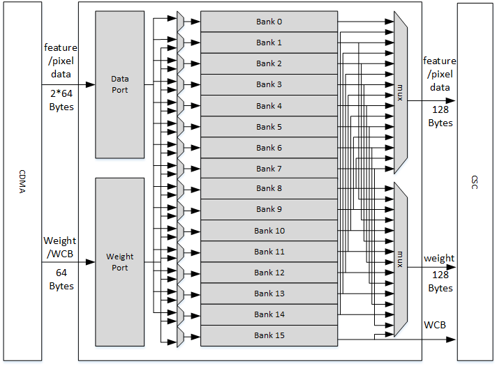
Fig. 52 Convolution buffer
Power Consideration
The Convolution Buffer applies clock gating for registers in the data path beyond the SRAMs. The clock of Convolution Buffer data path is gated by SLCG when it is idle and no HW-layer is available from the programmable registers. The configuration register block inside the convolution buffer is not clock gated so that a new configuration can be programmed.
Convolution Sequence Controller
Overview
The Convolution Sequence Controller (CSC) is responsible for loading input feature data, pixel data, and weight data from CBUF and sending it to the Convolution MAC unit. It’s the key module computing and controlling the convolution sequence descrbied in the Convolution Pipeline seciton.
The Convolution Sequence Controller (CSC) includes three sub modules: CSC_SG, CSC_WL and CSC_DL. See Fig. 53.
CSC_SG is the convolution sequence generator. This module generates the sequence to control convolution operation.
The working flow of CSC_SG is as below:
Poll for enough data and weights in CBUF
Generate a pair of sequence package, including weight loading package and data loading package. Each package represents one stripe operation.
Push the two packages into two FIFOs
Two counters for weight and feature/pixel are both down counting
When the counters reach zero, check signals from the convolution accumulator for any back pressure
If all conditions are ready, send weight and data packages in proper time to CSC_WL and CSC_DL.
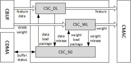
Fig. 53 Convolution sequence controller
CSC_DL is the convolution data loader. This module contains the logic to execute the feature/pixel loading sequence. It receives packages from sequence generator, loads feature/pixel data from CBUF and sends them to the Convolution MAC. It also maintains the data buffer status and communicates with CDMA to keep the status up to date. For winograd mode, it also performs PRA (pre-addition) to transform the input feature data.
CSC_WL is short of convolution weight loader. This module contains the logic to execute the weight loading sequence. It receives packages from the sequence generator, loads weights from CBUF, and does necessary decompression and sends them to convolution MAC. It maintains the weight buffer status and communicates with CDMA_WT to keep the status up to date.
Power Consideration
The Convolution Sequence Controller applies clock gating for registers in the data path. The clock of data path for the convolution sequence controller is gated when idle and no HW-layer is available from the programmable registers. The register file sub module inside convolution sequence controller is not clock gated so that new
Convolution MAC
Overview
The Convolution MAC (CMAC) module is one stage of the convolution pipeline for convolution operation. It receives input data and weight from the convolution sequence controller (CSC), performs multiplication and addition, and outputs the result to the convolution accumulator. When working in Winograd mode the Convolution MAC performs POA (post addition) on the ouptut to transform the result back to standard activation format.
CMAC has 16 identical sub modules called MAC cells. Each MAC cell contains 64 16-bit multipliers for int16/fp16. It also contains 72 adders for int16/fp16 which are for Winograd POA. Each multiplier and adder can split into two calculation units for int8 format. The throughput of int8 is twice of int16 in any mode. The output result is called partial sum. The pipeline depth is 7 cycles.
One bypassed pipeline in Convolution MAC is used to deliver status. The status includes start and end operation flags. It takes status 4 cycles to go through pipeline, which is 3 cycles ahead of partial sum to prefetch assembly buffer in CACC.
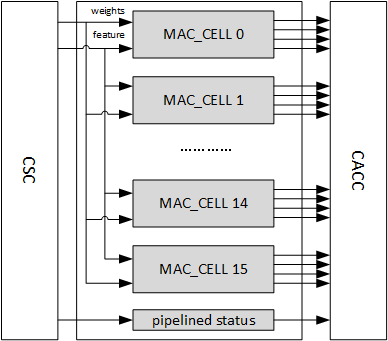
Fig. 54 Convolution MAC
For physical design optimization the CMAC is divided into two parts, CMAC_A and CMAC_B. Each part has an individual CSB interface and register file. But they are considered as one pipeline stage in usage.
Power Consideration
The clock of data path of the Convolution MAC is gated when it is idle and no hardware layer is available from the programmable registers. The the programmable registers are not clock gated in the Convolution MAC so that software can program
Besides, convolution MAC can clock gate the MAC cells individually. When the number of kernels is not enough to fill all the MAC cells, the empty ones will be automatically clock gated.
Convolution Accumulator
Overview
The Convolution Accumulator (CACC) is the stage of the convolution pipeline after CMAC. It is used to accumulate partial sums from Convolution MAC, and round/saturate the result before sending to SDP. Additionally, the large buffer in the convolution accumulator can smooth the peak throughput of the convolution pipeline.
The final result of accumulator in CACC is 48bits for INT16 and 34bits for INT8. The bit width between CACC and SDP is 32. For precisions INT8 and INT16, there is a round and saturation operation before sending the result to SDP. The precision of rounding is configured by field CLIP_TRUNCATE in register D_CLIP_CFG. For FP16, the value is just converted from FP48 to FP32.
The components in CACC include assembly SRAM group, delivery SRAM group, adder array, truncating array, valid-credit controller and a checker.
Here is the CACC working flow:
Prefetch accumulative sums from the assembly SRAM group.
When partial sums arrive, send them to adder array along with accumulative sums. If the partial sums are from the first stripe operation, the accumulative sums should be 0.
Gather new accumulative sums from output side of adder array.
Store into assembly SRAM group
Repeat step1~ step3 in terms of stripe operation until a channel operation is done.
If a channel operation is done, the output of adders is rounded and saturated.
Gather results of previous step and store them into delivery SRAM group.
Load results from delivery buffer group and send them to SDP
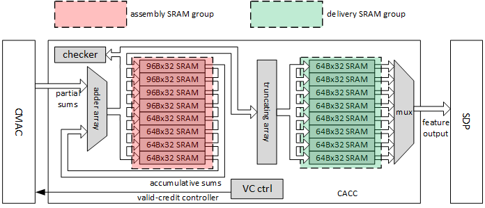
Fig. 55 Convolution accumulator
The assembly SRAM group contains 4 96Bx32 SRAMs and 4 64Bx32 SRAMs. The buffer group is used to cache accumulative sums with high precision. For direct convolution, assembly SRAM group acts as one 96Bx128 buffers for int16/fp16 or one 136Bx128 buffer for int8. For Winograd convolution, assembly SRAM acts as one 384Bx32 buffer for int16/fp16 or one 544Bx32 buffer for int8. It takes at least 11 cycles to do a read-store circle for assembly group.
The delivery SRAM group contains 8 64Bx32 SRAMs. The buffer group is used to cache the result to be delivered to SDP. The input varies from 16 elements to 128 elements per cycle, while the output is always 16 elements per cycle.
The precision of accumulative sum is as below.
Input Format |
Accumulative Sum |
Truncated Result |
|---|---|---|
INT8 |
INT34 |
INT32 |
INT16 |
INT48 |
INT32 |
FP16 |
FP44 (8b exponent, 38b signed decimal) |
FP32 (IEEE754 standard) |
In adder array, there are 64 INT48 adders, 64 INT34 adders and 64 FP48 adders. Part of them are activated in different mode
Input Format and Mode |
Activated INT48 Adders |
Activated INT34 Adders |
Activated FP44 Adders |
|---|---|---|---|
INT8 DC/Image |
Adder 0~15 |
Adder 0~15 |
NA |
INT8 Winograd |
Adder 0~63 |
Adder 0~63 |
NA |
INT16 DC/Image |
Adder 0~15 |
NA |
NA |
INT16 Winograd |
Adder 0~63 |
NA |
NA |
FP16 DC/Image |
NA |
NA |
Adder 0~15 |
FP16 Winograd |
NA |
NA |
Adder 0~63 |
To support multi-batch option in DC mode, CACC applies data remapping function in delivery SRAM group. That means when multi-batch is enabled, the data ordering in delivery SRAM group may not match the sequence from assembly SRAM group. Write controller of delivery SRAM will combine atomic cubes if they will be in same 64 bytes package after further calculation in SDP. This function allows SDP to send 64B aligned write requests as many as possible when multi-batch is enabled. Below diagram shows a case with batch size of 2.
Fig. 56 Data remapping in CACC
The protocol between CMAC and CACC is valid-only protocol. In case of overflow, CACC uses valid-credit protocol to back pressure CSC.
Power Consideration
The Convolution Accumulator applies clock gating in the data path. The clock of data path of Convolution Accumulator is gated when it is idle and no HW-layer is available from programmable registers. The programmable registers within CACC aren’t clock gated to allow for new instructions to be programmed.
Single Point Data Processor
Overview
The Single Point Data Processor (SDP) is performs post processing operations at the single data element level. In NVDLA version 1.0, point processing is designed to accomplish following operations.
Bias Addition
For a convolutional layer, there’re always a bias addition after convolution. In NVDLA, we implement bias addition in SDP.
The mathematic formula for bias addition is:
x is the input data can either come from Convolution Pipeline or SDP M-RDMA;
bias is a pre-trained parameter which can be one of 3 options:
Register: If bias is unique for entire data cube;
SDP B/N/E-RDMA per-channel mode: If bias is shared for all elements in the same channel;
SDP B/N/E-RDMA per-element mode: If bias is different element-by-element;
Non-Linear Function
The Non-Linear function hardware in SDP is used to accomplish activation layer operations.
Based on current network analysis, there are three activation functions are commonly used:
ReLU, for an input \(x\), the output is \(max(x,0)\).
Sigmoid, for an input \(x\), the output is \(\frac{1}{1 + e^{- x}}\).
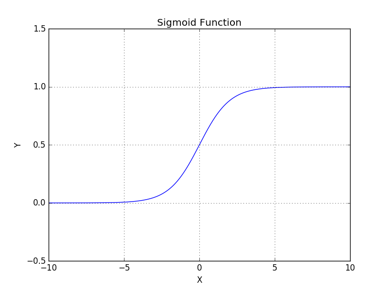
Fig. 57 Sigmoid Function
Hyperbolic tangent, for an input \(x\), the output is \(\frac{1 - e^{- 2x}}{1 + e^{- 2x}}\).
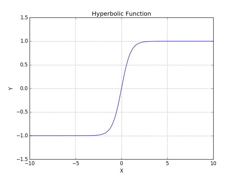
Fig. 58 Hyperbolic Tangent Function
In the case of the ReLU activation function, it could be implemented directly by hardware logic. Sigmoid and hyperbolic tangent functions are non-linear functions, so they are expected to be implemented through a look-up table which can be loaded with a function as needed. (see the Section “LUT programming” of Programming Guide document for details).
Batch Normalization
Batch normalization a is widely used layer. It can be descripted by formula below:
Where, \(\mu\) is the mean and \(\theta\) is the standard variance and x is element of feature data cubes.
SDP support batch normalization with given mean/standard variance parameters. The parameters are obtained from training.
SDP can support per layer parameter or per channel parameter to do batch normalization operation. When the parameter is per channel, they are interleaved in memory (see Data Formats). And a DMA in SDP will fetch the parameter and calculate the feature data cube from the convolution pipeline.
Element-Wise Layer
An Element-Wise layer refers to a type of operation between two feature data cubes which have the same W, H and C size. These two W x H x C feature data cubes do element-wise addition, multiplication or max/min comparison operation and output one W x H x C feature data cube.
Fig. 59 Element-wise operation
The SDP unit can support element-wise layers for all 3 types of data precisions. Every element-wise layer on SDP is configured to do addition or multiplication.
SDP supports both online mode and offline mode for element-wise layer. When online mode, one data cube comes from convolution pipeline, and the other input data cube is fetched from memory. When offline mode, SDP fetches both input data cubes from memory.
PReLU
Different from ReLU which clip negative values to 0, PReLU acts as:
Fig. 60 PReLU
The scaling factor k can be either per cube constant or per-channel variant.
SDP supports it by update the multiplier behavior: If PReLU mode is selected, multiplier will bypass the positive value and apply scaling on negative values only. PReLU mode is supported by a multiplier in all the 3 sub-modules.
Note that:
1. BatchNorm and PReLU feature are exclusive for a specific sub-unit, this is due to only one multiplier is available for a subunit;
2. If PReLU is enabled for one sub-unit, the ALU in that unit MUST be bypassed. This is due to there’s only one truncate for a sub-unit and negative/positive requires different truncate here.
Format conversion
NVDLA supports INT8, INT16, and FP16 precisions. Lower precision delivers higher performance, while higher precision provides better inference results.
It’s possible that software requires different precision for different hardware layers thus precision conversion is necessary.
SDP is responsible for precision conversion. The supported conversions in one hardware layer are listed in Table 30, “precision conversion for SDP layer (offline)”. If SDP sources data from the convolution core, the supported format conversion is listed in Table 29.
Precision conversion and normal SDP function are independent, which means SDP is able to do conversion and operation (e.g.: Bias addition, BatchNorm, EW, etc) at the same time.
Comparison
Comparison mode in SDP_Y takes 2 inputs then compares them. If any element pair from the input data cubes mismatches, a status register is updated after the hardware layer is complete.
To save bandwidth, there won’t be any output write to external memory in comparison mode.
Function Description
Following diagram shows the internal blocks of the point processing sub-unit and connections to other sub-units.
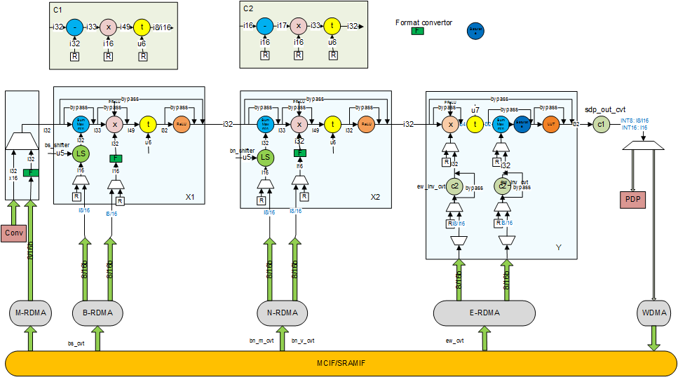
Fig. 61 Single point Data Processing block diagram
Function Blocks:
There are several function blocks, each of which targets a different purpose:
Block M is used to select input data from MEM or Conv Core, which can be set from register
Block X1/X2 have the same architecture and supports: Bias addition, BatchNorm, PReLU, ReLU, Eltwise.
Block Y is primarily designed for element-wise, but it’s also able to support Bias addition, PReLU. An extra LUT operation which can be selected before output to implement any non-linear operation.
Block C1/C2 is for additional scaling and offset to save bits while keeping accuracy high.
A Demux on the very end to send the output data to either WDMA for writing back to memory, or to PDP for a subsequent pooling operation.
Most of function units have a configurable bypass mode so SW can choose full function or partial to match all the operations needed in one hardware layer.
The throughput for each sub-unit is:
Sub-unit |
Throughput |
|---|---|
X1/X2 |
16 elements/cycle |
Y |
4 elements/cycle |
Working Mode: Flying:
On-flying: source data is from Conv-Core
Off-flying: source data is from Memory, which is read by M-RDMA
Bias Addition:
Operand data can be per element, per channel or per cube, the actual operation can be performed at any of X1/X2/Y based on software configuration
Bias data will be fetched from MEM if per element/channel. If truncate is enabled, all elements shares a same truncate value
Bias data will be set by register if per cube
Multiplier will be bypassed
Batch Normalization
Operand data can be per element, per channel or per cube, the actual operation can be performed in X1/X2/Y based on the software configuration.
Operand data will be fetched from MEM if per element/channel. If truncate is enabled, all elements shares a same truncate value.
Operand data will be set through a software configuration register if per cube.
Operand data for the adder and multiplier should be packed together and in same format of per element, per channel or per cube. See Data Formats for details.
ReLU can be bypassed or enabled.
Element-Wise
Operand data can be per element, per channel or per cube
Operand data will be fetched from MEM if per element/channel, if truncate is enabled, all elements shares a same truncate value
Operand data will be set by software configuration register if per cube
Operand data should be either for max/min/sum, or for the multiplier
LUT can be bypassed or enabled
PReLU:
Operand data can be per channel or per cube
Operand data will be fetched from MEM if per channel, if truncate is enabled, all elements shares a same truncate value
Operand data will be set by register if per cube;
PReLU mode bit should be set as true for multiplier. After this bit is set, hardware will bypass positive input samples, and the scaling will be applied on negative iputs.
LUT can be bypassed or enabled
Hybrid Mode (SW feature)
Bias addition/BatchNorm operations are linear operations. This means software can fuse those operation into one sub-module to optimize power/perf. Take BiasAddition + BatchNorm for example, if they’re working on separated submodule, the formula is: \(x^{'} = x + bias\), \(y = \frac{x^{'} - \mu}{\theta}\).
If we fuse those 2 formulas as one: \(y = \frac{x + bias - \mu}{\theta} = \frac{x - (\mu - bias)}{\theta}\).
As \(\mu, \theta, bias\) are pre-trained parameters, software can fuse them into one cube thus it’s doable;
As a summary, the features supported by each sub-unit are listed in table below:
FeatureModule |
X1 |
X2 |
Y |
|---|---|---|---|
Bias addition |
Y |
Y |
Y |
BatchNorm |
Y |
Y |
Y |
Eltwise |
Y |
Y |
Y |
PReLU |
Y |
Y |
Y |
ReLU |
Y |
Y |
Y |
Non-linear activation |
N |
N |
Y |
Data Sequence:
Take BIAS addition as an example, If BIAS/Operand Data is per element:
Point processing input/output sequence is determined by the convolution output sequence. In most of cases, input and output sequence orders in all input/output interfaces are the same, and it is exactly the convolution output sequence which is shown in the following diagram.
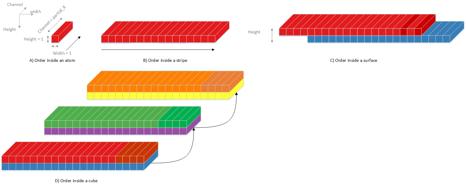
Fig. 62 Point processing input/output sequences
Bias/Operand Data is Per Channel:
Data will be fetched from memory, and maintain one value for multiple cycles when feature data is processing on the same surface. It will then update to the value of the next surface when feature data changes to the next surface.
Bias/Operand Data is Per Cube:
Data will be set in a software configuration register, and will not change throughout the execution time for a hardware layer.
Buffer Size Estimation
There are three major buffers in the single data processing subunit: LUT in the activation block, read DMA buffer, and write DMA buffer. LUT size is (65+ 257) *2(BPE) = 644Bytes.
For feature read DMA buffer in the M block there are two constraints to consider to determine its size. One is covering internal SRAM access latency. The latency is expected to be about 128 cycles. The other is access bandwidth. Each partial feature data element is 16 bits, and SDP needs to process 16 elements per cycle, so the required bandwidth is 32 bytes. The read DMA buffer size is therefore\(128 \times 32 = 4\ KBytes\).
Unlinke feature data, if BS/BN/EW has to support BatchNorm mode which has 32bits per element. Thus the read DMA buffer size for those 2 modules are: 32(bits)*128(cycles)*16(elements)/8=8Kbytes.
Power Consideration
Element-Wise/BatchNorm operation are not always included in a given network. So for uch of the operations, BS/BN/EW are not fully running thus clock gating is utilized.
Planar Data Processor
Overview
The Planar Data Processor (PDP) executes operations along the width x height plane. In NVDLA version 1.0, the PDPD is designed to accomplish pooling layers. Max, min, and mean pooling methods are supported. Several neighboring input elements within a plane will be sent to a non-linear function to compute one output element. The following diagram shows an example for max-pooling. The maximum value among 3x2 neighboring elements is the pooling result value.
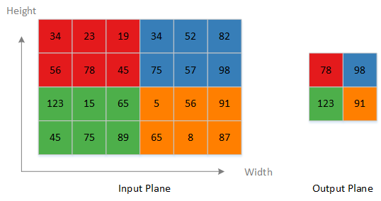
Fig. 63 Max-pooling example
The following diagram shows the internal blocks of the PDP sub-unit, along with connections to other units and sub-units. The diagram is captures the functionality conceptually and is does not show the actual RTL modules and hierarchies. The planar data processing sub-unit receives data from SDP or MCIF/SRAMIF, and sends data to MCIF/SRAMIF.
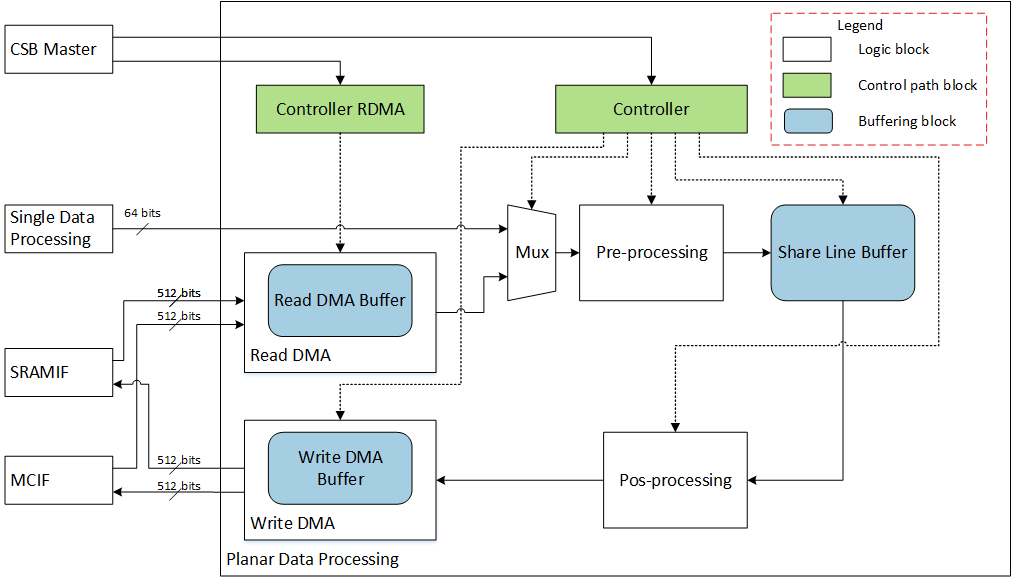
Fig. 64 Planar processing block diagram
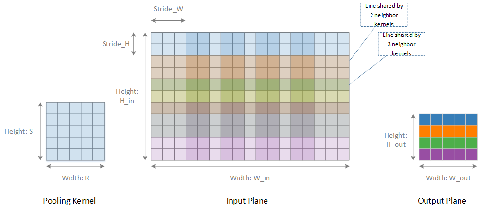
Fig. 65 Processing flow in one plane
Pooling operations are done within a plane. There is no interference between different planes. Fig. 66 shows a complete scheme of pooling in one plane. The offset of two neighboring kernels is called stride. When stride is less than R and S of a kernel, there are overlapped lines. Some line may be used by more than two neighboring kernels. Input data is streamed in raster-scan order. For each pooling kernel, the operated data is also streaming in raster scan order.
If an input data element is the first element of a kernel, it will be stored to the share line buffer. Data in the share line buffer is referred to as the partial result. If an input data element is neither the first element nor the last element of a kernel, it will be operated on with the existed partial result from share buffer, and the result will be stored to the same entry of the original partial result. Partial result calculation is done in the pre-processing block.
In cases of max/min pooling schemes, the partial result is the maximum/minimum value of the input element and the original partial result.
In case of mean pooling scheme, the partial result is the sum of the input element and the original partial result.
If an input data element is the last element of a kernel, it will be operated with the existed partial result from the share line buffer to generate a pre-final result. The post-processing block will fetch pre-final results from share line buffer, and after proper operations it generates the final result. This final result is sent out to SRAMIF or MCIF.
In cases of max/min pooling schemes, the pre-final result is the final result, no extra operation is needed.
In case of mean pooling scheme, the final result could be calculated by \(pre\_ final\_ result \times \frac{1}{\text{Kerne}l_{\text{width}} \times Kernel_{\text{height}}} = pre\_ final\_ result \times scale\_ factor\_ width \times scale\_ factor\_ height\). Division is expensive for a hardware implementation, so a pair of \(scale\_ factors\) are used to transform division into multiplication.
The greatest number of kernels which share the same line of data is determined by \(\text{ceiling}\left( \frac{Kernel\_ Height}{Stride\_ H} \right)\). The total buffer entry number needed within a plane is \(width\_ out \times ceiling\left( \frac{Kernel\_ Height}{Stride\_ H} \right)\) , and in the RTL design the assigned total buffer entry number \(total\_ buf\_ entry\) within one plane is as below, and 112 bits for each entry:
if \(\text{ceiling}\left( \frac{Kernel\_ Height}{Stride\_ H} \right)\) = 1, \(total\_ buf\_ entry\)=16*4*8=512;
if \(\text{ceiling}\left( \frac{Kernel\_ Height}{Stride\_ H} \right)\) = 2, \(total\_ buf\_ entry\)=16*4*4=256;
if \(\text{ceiling}\left( \frac{Kernel\_ Height}{Stride\_ H} \right)\) = 3 or 4, \(total\_ buf\_ entry\)=16*4*2=128;
if \(\text{ceiling}\left( \frac{Kernel\_ Height}{Stride\_ H} \right)\) > 4, \(total\_ buf\_ entry\)=16*4*1=64;
Since the pooling operation is a down sampling method, there is a significant amount of information are discarded. Pooling in a large kernel is too destructive. In current analyzed networks, there are three most common cases, one is pooling size 3x3, with stride 2x2. The other is pooling size 2x2, with stride 2x2, and the last is pooling size is 3x3, with stride 1x1. There are two other less used cases: one is pooling size 3x3, with stride 3x3. And the other is pooling size 7x7, with stride 1x1.
Network |
Total Pooling Layer Number |
size 3x3 stride 2x2 Number |
size 2x2 stride 2x2 Number |
size 3x3 stride 1x1 Number |
Other Layer Number |
Other Layer Pooling Format |
|---|---|---|---|---|---|---|
AlexNet |
3 |
3 |
0 |
0 |
0 |
NA |
Overfea t-Accur ate |
3 |
0 |
1 |
0 |
2 |
size 3x3 stride 3x3 |
VGG 19 |
5 |
0 |
5 |
0 |
0 |
NA |
GoogLeN et |
14 |
4 |
0 |
9 |
1 |
size 7x7 stride 1x1 |
NVDrive Net@960 x540 |
12 |
3 |
0 |
9 |
0 |
NA |
So 2 ~ 8 pooling kernel size (both in width and height) range and 1~8 stride range is enough for normal usage. In the RTL design, we set the pooling kernel size range to 1~8, and set the stride range to 1 ~ 16.
There are two input paths for the planar data processing sub-unit. One is the single point data processing sub-unit, and the other is external RAM (MC/SRAM). There is one output data path for planar processing sub-unit. Output data is always sent to RAM outside PDP (MC/SRAM). In common practice, a pooling layer is inserted after a convolutional layer. To save memory accessing consumptions, the planar data processing sub-unit shall directly receive data from point processing unit if following condition is met. Suppose output width is \(\text{Width}_{\text{output}}\), total buffer size in byte is \(\text{Size}_{\text{buffer}}\), overlapped line number \(\text{Num}_{overlapped\_ line}\), Data width in byte is \(\text{Data}_{\text{width}}\), the number of spatial plane is called ongoing channel number \(\text{Num}_{ongoing\_ channels}\), normally, \(\text{Num}_{ongoing\_ channels}\) should be equals to kernel_per_group (16 for INT16/FP16, 32 for INT8 pipe). Below is the planar processing on-fly operation condition.
If \(\text{ceil}\left( \frac{\text{Height}_{\text{poolin}g_{\text{kernel}}}}{\text{Strid}e_{h}} \right) = 1\) , \(f\left( \text{ceil}\left( \frac{\text{Height}_{\text{poolin}g_{\text{kernel}}}}{\text{Strid}e_{h}} \right) \right) = 1\)
If \(\text{ceil}\left( \frac{\text{Height}_{\text{poolin}g_{\text{kernel}}}}{\text{Strid}e_{h}} \right) = 2\) , \(f\left( \text{ceil}\left( \frac{\text{Height}_{\text{poolin}g_{\text{kernel}}}}{\text{Strid}e_{h}} \right) \right) = 2\)
If \(\text{ceil}\left( \frac{\text{Height}_{\text{poolin}g_{\text{kernel}}}}{\text{Strid}e_{h}} \right) = 3\ or\ 4\) , \(f\left( \text{ceil}\left( \frac{\text{Height}_{\text{poolin}g_{\text{kernel}}}}{\text{Strid}e_{h}} \right) \right) = 4\)
If \(\text{ceil}\left( \frac{\text{Height}_{\text{poolin}g_{\text{kernel}}}}{\text{Strid}e_{h}} \right) > 4\) , \(f\left( \text{ceil}\left( \frac{\text{Height}_{\text{poolin}g_{\text{kernel}}}}{\text{Strid}e_{h}} \right) \right) = 8\)
When input data is sourced from the point processing sub-unit, the input data sequence is the same as convolution output sequences which is shown in following diagram.
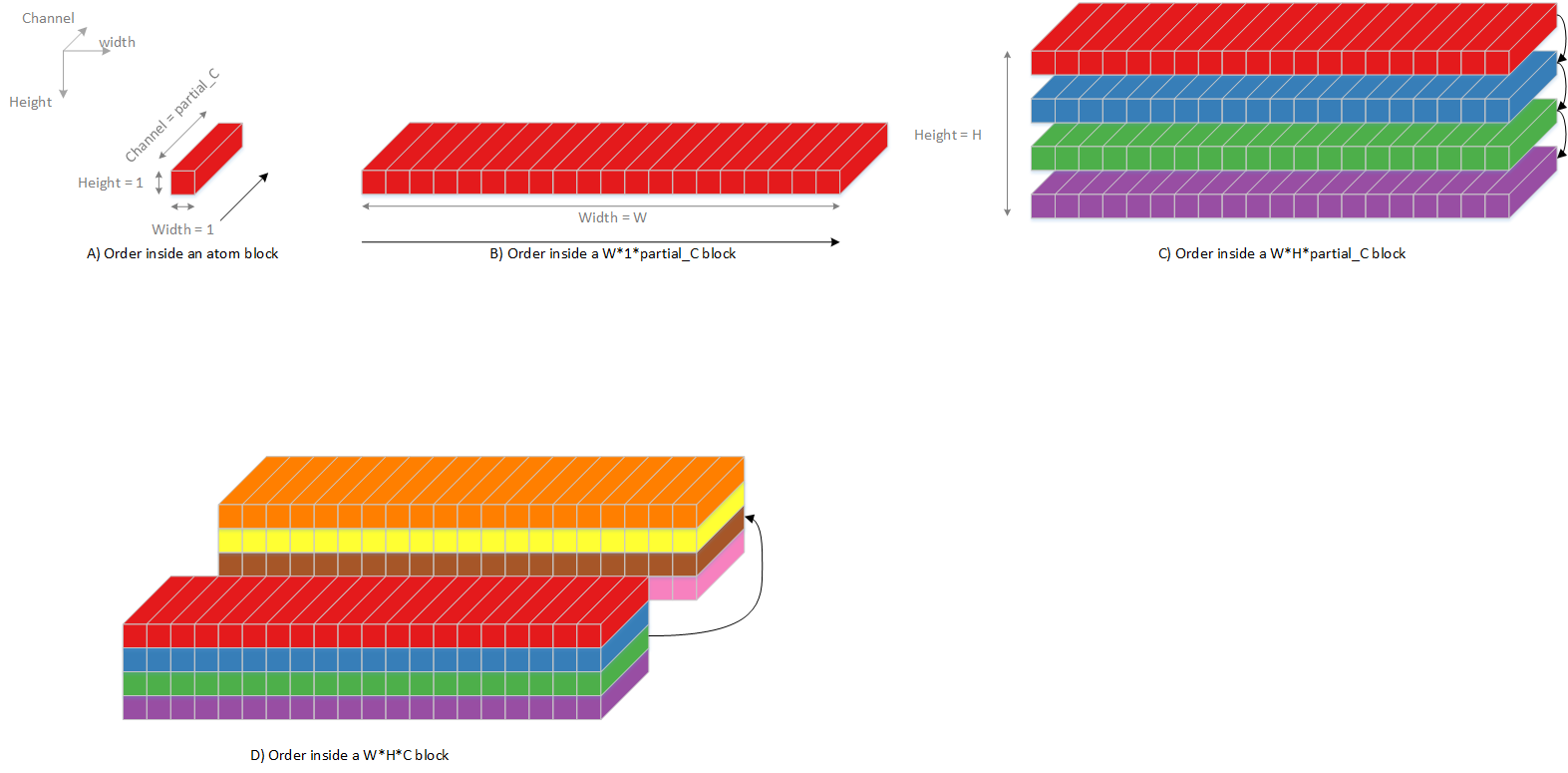
Fig. 66 Planar processing input sequence, mode 0
And output sequence is shown in following diagram.
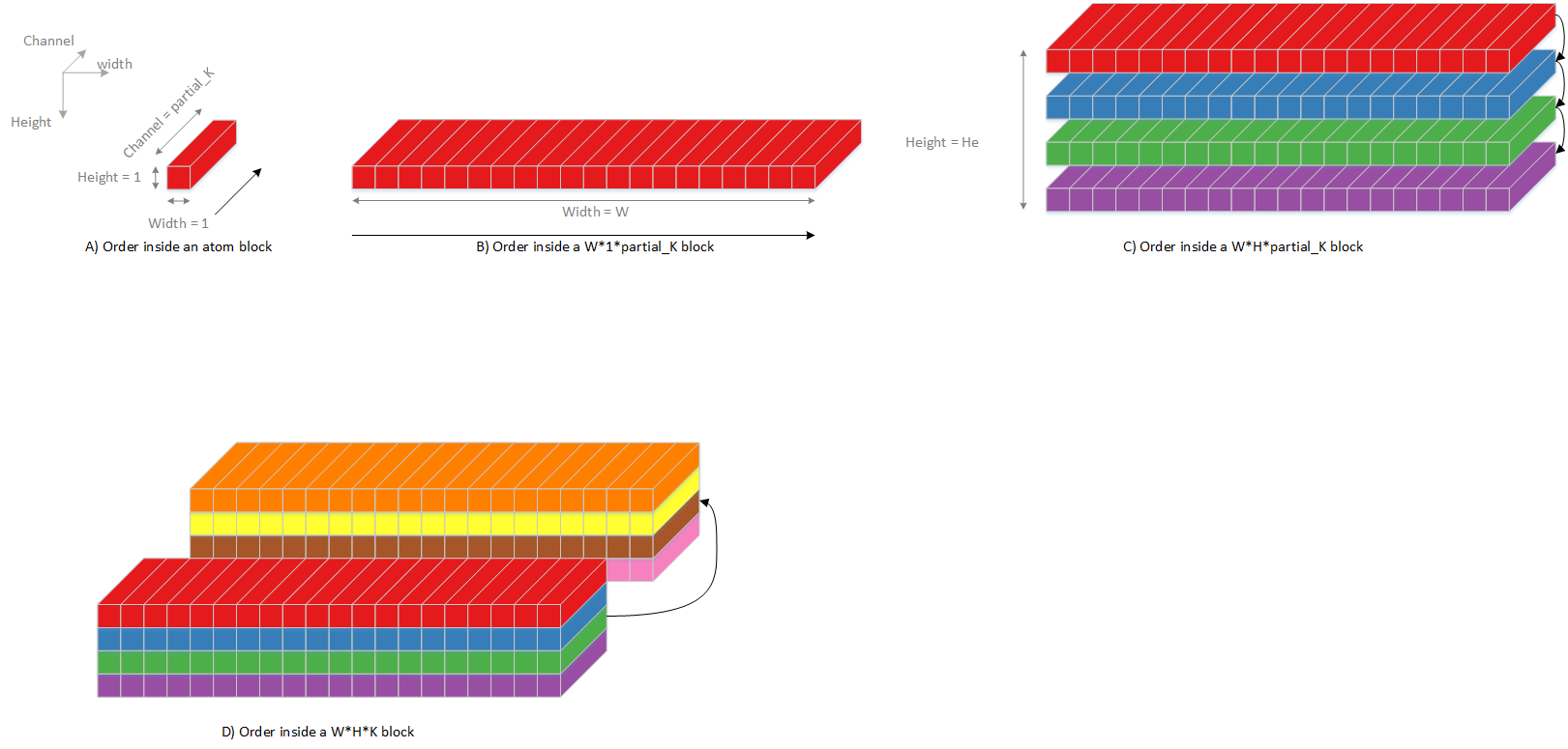
Fig. 67 Planar processing output sequence, mode 0
If planar processing on-the-fly operation condition is not meet, planar processing shall work in off-fly mode, it receives data from PDMA, and the ongoing channel number is always 16. There are two sub-cases, one is non-split-width, and the other is split-width. The input data sequence is shown in following diagram.
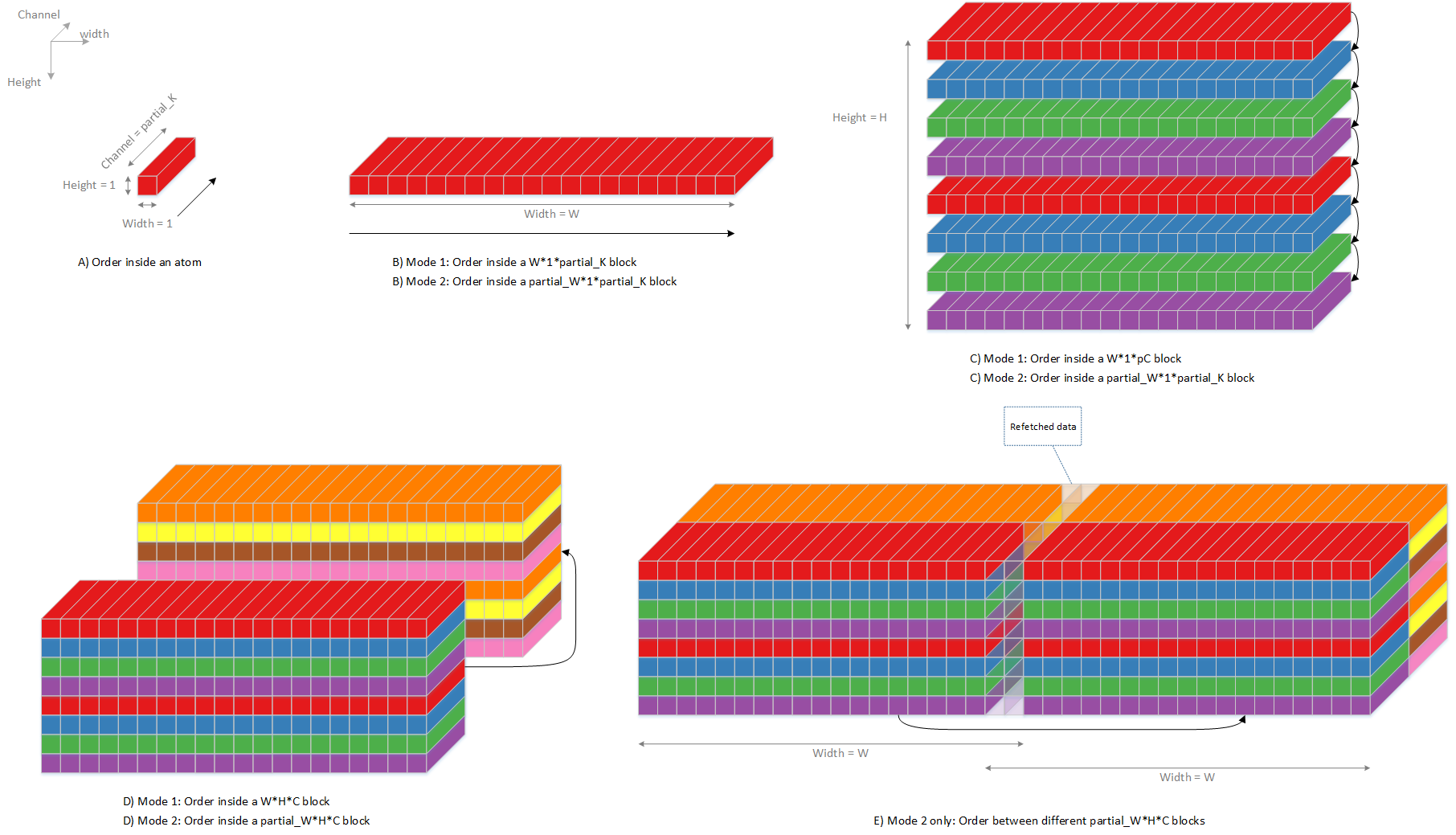
Fig. 68 Planar processing input sequence, mode 1 and 2
The output data sequence is shown in following diagram.
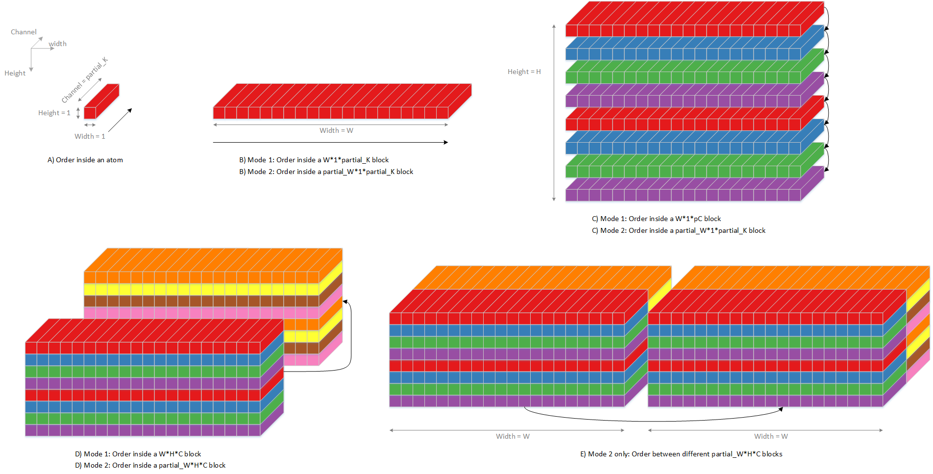
Fig. 69 Planar processing output sequence, mode 1 and 2
Operation mode |
Data Source |
Split-Width |
|---|---|---|
Mode 0 |
Single-point Data Processing |
No |
Mode 1 |
MC/SRAM |
No |
Mode 2 |
MC/SRAM |
Yes |
Buffer Size Estimation
There are three major buffers in planar data processing subunit: share line buffer, read DMA buffer, and write DMA buffer. For share line buffer, its size determines whether PDP could work directly on data from SDP or not. Based on input data cube height \(\text{Height}_{\text{input data cube}}\), pooling kernel height \(\text{Height}_{\text{pooling kernel}}\), pooling kernel stride in height direction \(\text{stride}_{\text{pooling kernel}}\), output data cube width \(\text{Width}_{\text{output data cube}}\), group size (16 elements of int16/FP16 or 32 elements of int8, ~32 byte) \(\ \text{Group}_{\text{size}}\) and bytes_per_element(14/8 for INT8, 28/8 for INT16, 28/8 for FP16).
If the share line buffer capacity is less than the required consumption size, PDP have to work in off-fly mode, so there will be a performance drop since extra-time is needed to store data to MC/SRAM, and then fetch back to PDP for pooling processing.
Layer |
Channel Number |
Kernel Size |
Kernel Stride |
Output Width |
Minimum Size |
Maximum Size |
|---|---|---|---|---|---|---|
AlexNet – pool1 |
96 |
3 |
2 |
27 |
1728 |
5184 |
AlexNet – pool2 |
128 |
3 |
2 |
13 |
832 |
3328 |
AlexNet – pool5 |
128 |
3 |
2 |
6 |
384 |
1536 |
Overfea t-Accur ate – layer 3 |
96 |
3 |
3 |
36 |
1152 |
6912 |
Overfea t-Accur ate – layer 6 |
256 |
2 |
2 |
15 |
480 |
7680 |
Overfea t-Accur ate – layer 19 |
1024 |
3 |
3 |
5 |
160 |
10240 |
VGG 19 – pool1 |
64 |
2 |
2 |
112 |
3584 |
14336 |
VGG 19 – pool2 |
128 |
2 |
2 |
56 |
1792 |
14336 |
VGG 19 – pool3 |
256 |
2 |
2 |
28 |
896 |
14336 |
VGG 19 – pool4 |
512 |
2 |
2 |
14 |
448 |
14336 |
VGG 19 – pool5 |
512 |
2 |
2 |
7 |
224 |
7168 |
GoogLeN et - pool1/3 x3_s2 |
64 |
3 |
2 |
56 |
3584 |
7168 |
GoogLeN et - pool2/3 x3_s2 |
192 |
3 |
2 |
56 |
3584 |
21504 |
GoogLeN et - incepti on_3a/p ool |
192 |
3 |
1 |
28 |
2688 |
32256 |
GoogLeN et - incepti on_3b/p ool |
256 |
3 |
1 |
28 |
2688 |
43008 |
GoogLeN et - pool3/3 x3_s2 |
480 |
3 |
2 |
14 |
896 |
13440 |
GoogLeN et - incepti on_4a/p ool |
480 |
3 |
1 |
14 |
1344 |
40320 |
GoogLeN et - incepti on_4b/p ool |
512 |
3 |
1 |
14 |
1344 |
43008 |
GoogLeN et - incepti on_4c/p ool |
512 |
3 |
1 |
14 |
1344 |
43008 |
GoogLeN et - incepti on_4d/p ool |
512 |
3 |
1 |
14 |
1344 |
43008 |
GoogLeN et - incepti on_4e/p ool |
528 |
3 |
1 |
14 |
1344 |
44352 |
GoogLeN et - pool4/3 x3_s2 |
832 |
3 |
2 |
7 |
448 |
11648 |
GoogLeN et - incepti on_5a/p ool |
832 |
3 |
1 |
7 |
672 |
34944 |
GoogLeN et - incepti on_5b/p ool |
832 |
3 |
1 |
7 |
672 |
34944 |
GoogLeN et - pool5/7 x7_s1 |
1024 |
7 |
1 |
1 |
224 |
14336 |
In the above table, most of the minimum cases are less than 7Kbytes. So as a result of balancing performance and the share line buffer size is set as 7Kbyte.
For read DMA buffer, there are two constraints for determining its size. One is covering MC accessing latency, assumed to be 128 cycles. The other is access bandwidth. The peak performance case is 8 Bytes per cycle (8 elements in int8, 4 elements in int16/fp16). So the read DMA buffer size is\(128 \times 8 = 1KBytes\).
Power Consideration
Planar processing sub-unit targets for pooling layer in NVDLA 1.0, based on analysis on current networks, planar processing usage is not expected to be high.
Network |
Total Pooling Layer Number |
Total Layer Number* |
Percentage |
|---|---|---|---|
AlexNet |
3 |
13 |
23% |
Overfeat-Accurate |
3 |
12 |
25% |
VGG 19 |
5 |
24 |
21% |
GoogLeNet |
14 |
74 |
19% |
* Total Layer Number = Convolution (including FC) + Pooling + LRN
Based on the pooling layer number percentage it’s highly likely that the planar processing sub-unit is idle most of the time. Sub-unit level clock gating is therefore important.
Cross Channel Data Processor
Overview
Cross Channel Data Processor (CDP) executes operations along channel direction. In NVDLA version 1.0, channel processing is designed to address local response normalization (LRN) layers. Local response normalization performs a kind of lateral inhibition by normalizing over local input region along the channel direction. The normalization function is shown as follow
Local region shape is always \(1 \times 1 \times n\). Number \(n\) is configurable, and its range is \(\lbrack 3,5,7,9\rbrack\). Arithmetic functions such as division and fractional exponents are expensive to implement with hard-wired gates. The above equation could be decomposed into
Be noticed the \(\sum_{i = max(0,c - \frac{n}{2})}^{min(C - 1,\ c + \frac{n}{2})}\text{Source}_{w,h,i}^{2}\) and \(\text{Source}_{w,h,c} \times f(x)\) can be bypassed by programming corresponding registers so that CDP can be treated as a standalone lookup table (LUT) function.
The Look-up table approach is adopted for the RESMO (reciprocation-exponent-sum-multi operation)\(f\left( x \right)\).
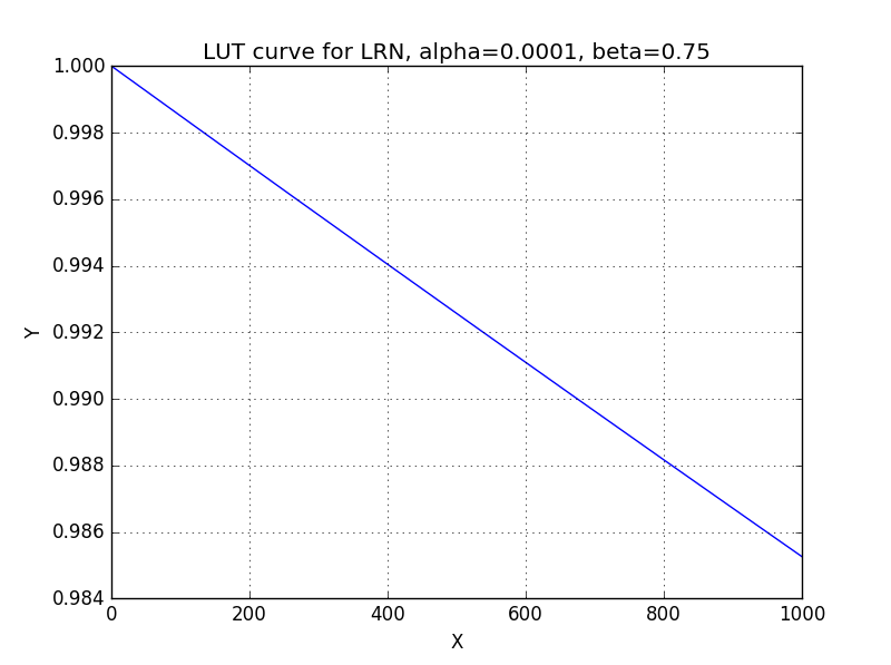
Fig. 70 Curve for reciprocation-exponent-sum-multi operation
The following diagram shows internal blocks of the channel data processing sub-unit and connections to other sub-units. The diagram is just for capturing ideas and does not represent the actual RTL modules boundaries and hierarchies.
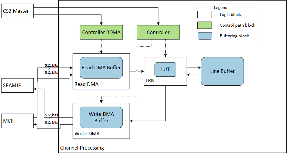
Fig. 71 Cross Channel Data Processing Block diagram
Channel processing sub-unit always works independently with other processing sub-units. It receives input data from and send output data to PDMA. Due to memory accessing constraint, the input data sequence is in a particular orders. The input sequence is shown in following diagram, and output sequence is the same as input sequence.
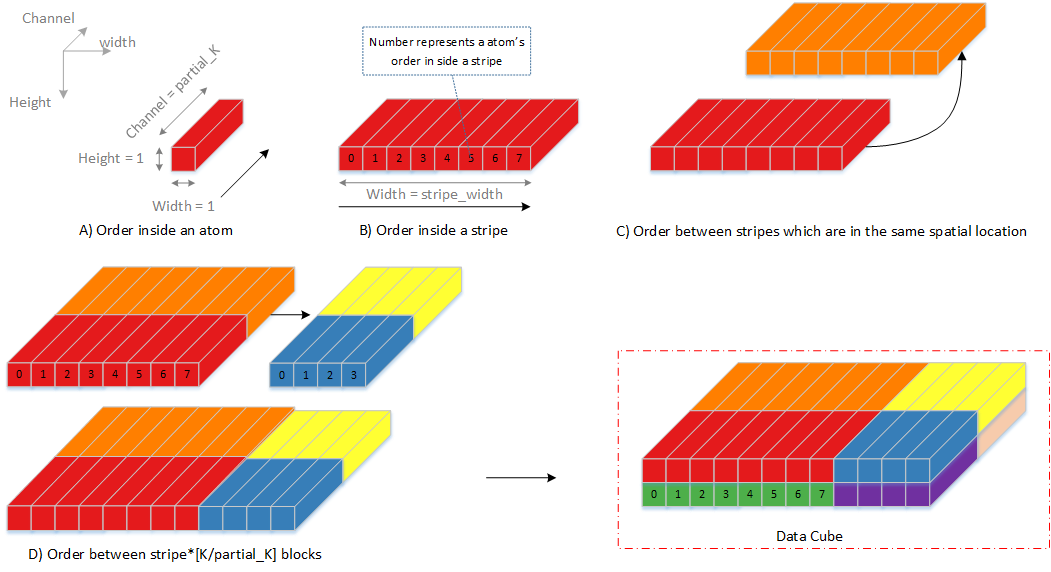
Fig. 72 Channel Processing input/output sequence
The following table shows LRN layers parameters in current well know networks.
Network |
Total LRN Layer Number |
Local Size Number |
Alpha |
beta |
|---|---|---|---|---|
AlexNet |
2 |
5 |
0.0001 |
0.75 |
Overfeat-Accurate |
0 |
NA |
0.0001 |
0.75 |
VGG-19 |
0 |
NA |
0.0001 |
0.75 |
GoogLeNet |
2 |
5 |
0.0001 |
0.75 |
Data elements on stripe edge may be used by to neighboring stripes. Those data needs to be buffered, buffer entry number shall be \(\left\lbrack \text{Max}\left( \text{loca}l_{\text{regio}n_{\text{size}}} \right) - 1 \right\rbrack \times 8 = 7 \times 8 = 56\ byte\).
Buffer Size Estimation
There are three major buffers in the cross-channel data processing subunit: LUT in the activation block, read DMA buffer, and write DMA buffer. The LUT size is the same as SDP (644Bytes).
For the read DMA buffer, there are two constraints for determining its size. The first is to cover memory system access latency. The assumption is 128 cycles. The other is access bandwidth. The peak performance case is 8 Bytes per cycle (8 elements in int8, 4 elements in int16/fp16), so the read DMA buffer size is \(128 \times 8 = 1KBytes\).
Power Consideration
The channel data processing sub-unit targets for LRN layer in NVDLA 1.0. Based on analysis of current networks, the channel processing usage is low.
Network |
Total LRN Layer Number |
Total Layer Number* |
Percentage |
|---|---|---|---|
AlexNet |
2 |
13 |
15% |
Overfeat-Accurate |
0 |
12 |
0% |
VGG 19 |
0 |
24 |
0% |
GoogLeNet |
2 |
74 |
3% |
* Total Layer Number = Convolution (including FC) + Pooling + LRN
Based on local response normalization layer number percentage the channel data processing sub-unit will be idle most of the time. Therefore, the design supports clock gating of the unit.
RUBIK
Overview
RUBIK module is similar to BDMA. It transforms data mapping format without any data calculation. RUBIK has 3 working modes, they are:
contract data cube
split feature data cube into multi-planar formats
merge multi-planar formats to data cube
Since the module’s function is to transform feature data cubes, we call it RUBIK unit.
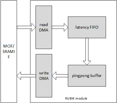
Fig. 73 RUBIK
Contract
A software deconvolution layer always uses several HW-layers or two phases. Phase I is generate result by convolution pipeline. And phase II is contract mode by RUBIK.
Normally, a SW deconvolution layer has deconvolution x stride and y stride that are greater than 1. And with these strides the output of phase I HW-layer is a channel-extended data cube. Contract mode in RUBIK transforms mapping format to de-extend the cube. The figure below shows a remapping example where the x stride is 2 and the y stride is 3.
Fig. 74 Contract mode in RUBIK
The formula of input cube size and output size are:
The RUBIK engine does contract slice by slice. It takes one Wx1xC input slice and converts it to a W’xH’xC’ output sub cube. Then it continues to the next input slice. It never sends a request across a line boundary.
When doing contract, the input/output start address and line stride shall align to 32 bytes. It always tries to send 256 byte requests. The memory efficiency is between 80%~100% which is affected by start address. If all address stride and start address are 256 byte aligned, the memory efficiency reaches 100%.
Requirement of contract mode:
The channel size shall be divisible by deconvolution x stride, y stride and 32 bytes. As formula below:
Each dimension of input and output data cube, like input data width, output data width, input channel size, should not exceed 8192 in one contract layer.
Split and Merge
Split and merge are two opposite operation modes in RUBIK. Split transforms a data cube into M-planar formats (NCHW). The number of planes is equal to channel size. The merge mode transforms a serial of planes to a feature data cube. The transform is showed in figure below.
Fig. 75 Split and merge modes in RUBIK
The M-planar format is similar to image formats. It’s a pitch linear format which contains T_R16_I, T_R8_I or T_R16_F data. Each plane contains only 1 channel data or single element. The line stride and planar stride of all planes(M-planar) shall align to 64 bytes. It’s unlike other data formats for NVDLA.
Power Consideration
The RUBIK unit applies clock gating in the data path. The clock of data path of RUBIK is gated when the unit is idle and no HW-layer is available from the programmable registers.
MCIF
MCIF is used to arbitrate requests from several internal sub modules and convert to AXI protocol to connect to external DRAM.
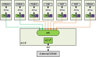
Fig. 76 MCIF
MCIF will support both a read and write channels, but some NVDLA sub-module will only have read requirement, so the interface between sub-module and MCIF will support read, write or both. CDMA0 and CDMA1 in the above diagram will need read only, and other 5 will need both read and write.
SRAMIF
The SRAMIF moduile is used to connect several internal sub-modules to on-chip SRAM. It’s similar to the MCIF but the bus latency is expected to be lower.
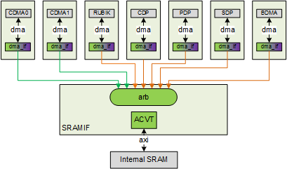
Fig. 77 SRAMIF
SRAMIF will support both read and write channels, but some NVDLA sub-modules will only have a read requirement, so the interface between DMA engines and SRAMIF will support read, write or both. CMDA0~1 will need read channel only, while the other 5 will need both read and write.
Result Statistics
To perform better calculation accuracy with limited precision data type like int8, NVDLA engine involved a large number of converters in many pipeline stages. Please see Section “Precision programming” of Programming Guide document for more detail.
In the runtime software, conversion parameters can be either a static value or a dynamic value. To support the latter ones, software requires NVDLA hardware to provide rough statistics of output feature data cube and calculate the parameters accordingly.
To achieve that, NVDLA implements result statistic registers in most pipeline stages. These registers record:
Number of results that is equals to max non-infinity values.
Number of INF/NaN on input port
Number of INF on output port
Based on these statistic record, SW can tell rough situation of output feature data cube and figure out proper parameters for next layer.
The pipeline stages involved in result statistic are:
Convolution DMA
Convolution accumulator
Single data processor
Planar data processor
Cross channel data processor
Here’s a list of statistic counting registers and its valid condition:
Register |
Valid condition |
|---|---|
CDMA. D_INF_INPUT_DATA_NUM CDMA. D_INF_INPUT_WEIGHT_NUM |
CDMA. IN_PRECISION==FP16 |
CDMA. D_NAN_INPUT_DATA_NUM CDMA. D_NAN_INPUT_WEIGHT_NUM |
CDMA. IN_PRECISION==FP16 |
SDP_RDMA.D_STATUS_NAN_INPUT_NUM SDP_RDMA. D_STATUS_INF_INPUT_NUM |
SDP_RDMA.IN_PRECISION==FP16 && SDP_RDMA.PERF_NAN_INF_COUNT_EN==YES |
SDP. D_STATUS_NAN_INPUT_NUM SDP. D_STATUS_INF_INPUT_NUM |
Not used |
SDP. D_STATUS_NAN_OUTPUT_NUM |
SDP.OUT_PRECISION==FP16 && SDP. PERF_NAN_INF_COUNT_EN=YES |
CDP. D_INF_INPUT_NUM CDP. D_NAN_INPUT_NUM CDP. D_NAN_OUTPUT_NUM |
CDP. INPUT_DATA_TYPE=FP16 |
PDP. D_INF_INPUT_NUM PDP. D_NAN_INPUT_NUM PDP. D_NAN_OUTPUT_NUM |
PDP. INPUT_DATA =FP16 |
Pipelines of NVDLA core
All sub units in NVDLA core logic is introduced in sections above. Some sub units are combined as one pipeline; some are working as individual pipelines. All of possible pipeline working modes are summarized in table below.
Pipeline Working Mode |
Sub Units |
Interface |
Support Layers |
|---|---|---|---|
Convolution pipeline |
CDMA, CBUF, CSC, CMAC, CACC, SDP |
MCIF/SRAMIF |
direct convolution, Winograd, image input layer, element-wise layer, batch-normaliza tion, activation (relu, prelu, sigmoid, etc.) layer |
Convolution & pooling pipeline |
CDMA, CBUF, CSC, CMAC, CACC, SDP, PDP |
MCIF/SRAMIF |
direct convolution + pooling layer (multi-batch mode is not supported) |
Offline SDP pipeline |
SDP |
MCIF/SRAMIF |
activation layer, element-wise layer, batch-normaliza tion layer, format conversion layer, comparison layer |
Offline PDP pipeline |
PDP |
MCIF/SRAMIF |
Pooling layer |
CDP pipeline |
CDP |
MCIF/SRAMIF |
LRN layer |
BDMA pipeline |
BDMA |
MCIF/SRAMIF |
Data transmission layer |
Rubik pipeline |
Rubik |
MCIF/SRAMIF |
Data transform layers |