Programming Guide
(Notice: This version of Unit Description is only for nvdlav1 release. Please refer to Scalability parameters and ConfigROM for other configurations)
BDMA programming
Background
We suggest NVDLA memory accesses are based on internal SRAM to achieve best performance and we designed BDMA for this purpose.
The supported memory transfers are:
Source type |
Destination type |
|---|---|
External DRAM |
Internal SRAM |
External DRAM |
External DRAM |
Internal SRAM |
External DRAM |
Internal SRAM |
Internal SRAM |
Programming
The programming model for BDMA is different from others due to special use scenario on BDMA. Take convolution as an example, in order to make a convolution layer operation happen, BDMA has to transfer input_feature/weight/mean/bias into internal SRAM. If BDMA also uses the traditional programming model, CPU will act as:
Issue setting for single transfer of input feature
Wait for interrupt
Issue setting for single transfer for weight
Wait for interrupt
…
The total time is:
4(Weight/Image/Mean/Bias) * CPU_ISR_Time + 4*TransactionTime;
This process is boring and many interactions between CPU and BDMA are needed. In order to improve the efficiency, a new programming model for BDMA is listed as below:
CPU issue setting for single transfer of input feature (set interrupt flag as false)
Pooling BDMA if there’s empty slot for program (BDMA support 20 register entries thus most of time, polling always return true)
CPU issue setting for single transfer of weight (set interrupt flag as false, if it’s not the last transfer request)
Repeat 2~3 until all data transfer request are done and set interrupt flag as true for last request
Wait for interrupt
The total time for outstanding based programming model is:
1*CPU_ISR_Time + 4*Transaction_Time;
We introduce 2 terminologies to describe procedure above:
Operation: Each individual BDMA transaction is called as operation. One operation may or may not trigger interrupt depending on software setting. take example above, transfer of activation, weight, mean, bias are 4 different BDMA operation.
Group: group is consisted by one or more BDMA operations depending on software configuration. Set GRP<0|1>_LAUNCH as YES is treated as end of a group.
During one BDMA group register programming, hardware acts as:
Software program one BDMA operation then set the EN bit
Hardware “cache” the corresponding BDMA registers to its internal slot, no actual memory transaction carried out. There’re totally 20 slots thus we can support 20 BDMA operations in one group as maximum;
Software poll the free slots by read STATUS.FREE_SLOTS, if it’s bigger than 0, it means software is allowed to program the next BDMA operation;
For the last BDMA operation in one group, software has to set CFG_LAUNCH<0|1>.GRP<0|1>_LAUNCH = YES;
Hardware will actually kick of all the “cached” BDMA operations in this group (by detect INTERRUPT=YES).
After all BDMA operation done, corresponding interrupt will be generated.
For below section, if there’s no special declaration, all address refers to data address in SRAM.
Buffer allocation
Before introduce buffer allocation formula, we need to understand the related register definition:
Register |
Description |
|---|---|
CFG_LINE |
Indicate the valid data size per line. This register should be configured as: valid_bytes_per_line/32-1 |
CFG_LINE_REPEAT |
Number of lines per surface. This register should be configured as: surface_height-1 |
CFG_SRC/DST_LINE |
Number of bytes per src/dst line (padding are included). It should be configured as: total_bytes_per_line |
CFG_SURF_REPEAT |
Number of surfaces in one data cube |
CFG_SRC/DST_SURF |
Number of bytes per surface (line padding are included). It should be configured as: total_bytes_per_surface |
Given the register definition above, the formula for buffer allocation are:
The formula for actual bytes transferred is: .. math:: actual_size = (CFG_LINE - 1) * 32 * CFG_LINE_REPEAT * CFG_SURF_REPEAT
Rubik programming
Features
Mode |
Description |
|---|---|
Contract |
Worked as final phase of deconvolution to reorder the output layout; |
Split |
Convert the feature format to M-planar format |
Merge |
Convert the M-planar format to feature format. |
Programming
Contract
Config the RUBIK_MODE= CONTRACT
Configure the input cube information:
D_DAIN_RAM_TYPE: The input memory type;
D_DATAIN_SIZE_0/1: The input W/H/C;
D_DAIN_ADDR_HIGH/LOW: The input cube start address;
D_DAIN_LINE/SURF_STRIDE: The input cube line/surface stride;
Configure the output cube information:
Register |
Value |
|---|---|
D_DATAOUT_SIZE_1 |
(DATAIN_CHANNEL+1)/(( DECONV_X_STRIDE+1)*( DECONV_Y_STRIDE+1))-1 |
D_DAOUT_ADDR_HIGH/LOW |
The output cube start address |
D_DAOUT_LINE/SURFACE_STRIDE |
The output cube line/surface stride |
D_CONTRACT_STRIDE_0 |
Ceil((DATAOUT_CHANNEL+1) * BPE / 32) * DAIN_SURF_STRIDE |
D_CONTRACT_STRIDE_1 |
(DECONV_Y_STRIDE+1) * DAOUT_LINE_STRIDE |
Configure the stride information:
D_DECONV_STRIDE: The x/y stride relationship between input/output cube. It’s not necessary to configure those values the same as deconvolution stride.
Configure the op_en to kick-off the hardware layer;
Split/Merge
Most of the configurations are the same as Contract mode except:
RUBIK_MODE should be SPLIT/MERGE;
D_DAIN_PLANAR_STRIDE has to be configured for merge mode;
Registers below are not necessary to program for split mode:
D_CONTRACT_STRIDE_0/1
D_DAIN_PLANAR_STRIDE
D_DAOUT_SURF_STRIDE
D_DECONV_STRIDE
Registers below are not necessary to program for merge mode:
D_CONTRACT_STRIDE_0/1
D_DAIN_SURF_STRIDE
D_DAOUT_PLANAR_STRIDE
D_DECONV_STRIDE
For split mode, DATAOUT_CHANNEL is used to specify number of channels needs to split thus it equals to output planar number.
Convolution pipeline programming
Features
From algorithm wise, convolution pipeline in NVDLA supports algorithm features below:
Feature |
Description |
|---|---|
Convolution |
Convolution layer functionality. It supports image input and feature input |
Deconvolution |
Deconvolution layer functionality; It supports feature input only. (Actually, deconvolution is a NVDLA software feature instead of hardware) |
Dilation |
A technology to expand kernel coverage without introduce more network parameters. |
Padding |
Padding size on the left/right/top/bottom of input data cube |
conv_stride |
The number of input element should be skipped in x/y direction after one output element be calculated |
From performance wise, convolution pipeline implements features below to accelerate convolution process:
Feature |
Description |
|---|---|
Winograd |
A fast convolution method (2.25x throughput than direct convolution), NVDLA support equivalent kernel size = 3x3 only (equivalent means kernel after channel extension) |
Channel Post-extension |
A method to improve MAC efficiency when channel size is too small (For image input only). |
Multi-Batch mode |
A method to improve MAC efficiency when atomic number in one stripe operation is too small (e.g.: InnerProduct layer). |
Weight compression |
A method to save weight data loading bandwidth. |
Besides hardware features, different working modes will impact performance as well:
Working mode |
Description |
|---|---|
Full input & weight |
If both weight/feature can be fitted to CONV_BUF, this mode delivers best performance |
Full input, partial weight |
If feature can be fitted to CONV_BUF while only part of weight can be fitted to CONV_BUF Comparing with full feature & weight, it has the same performance for single hardware layer, but weight can’t be re-used. |
Split H |
A software feature which utilize multiple HWLs to process an input data cube. It will be used when above cases are failed to match. |
Here’s the detailed explanation about those working modes:
Full input & weight mode
Condition: Both input feature and weight cube can be fitted in CONV_BUF
Fit case: small sized input/weight data
Data refetch: No
Weight refetch: No
Output sequence: K’(32 or 16)W HK
In this mode, entire input/weight will be loaded to CONV_BUF which means CONV_BUF should be large enough to store W*H*C+R*S*C*K data elements thus:
Full input, partial weight mode
Condition: Entire input feature data and part of weight data (2*kernel_per_group) can be filled in CONV_BUF
Fit case: small sized input and small/middle sized weight data
Data refetch: No
Weight refetch: No
Output sequence: K’(32 or 16)W HK
Full input feature mode is a most common case for many networks. Because the output sequence goes at K direction at last phase, it can be easily connected to pooling logic without big buffering requirement. Below formula should be satisfied when planning CONV_BUF layout:
The reason for 2*kernel_per_group is to keep CDMA and CMAC working at the same time to hide kernel loading latency, however, 1*kernel_per_group also workable but the performance is reduced.
Split H
We can see only full mode is supported by convolution pipeline. If one network layer has large input which exceed the CONV_BUF capacity, software has to split the big input cube into smaller cubes in vertical direction. This mechanism called “Split H mode”.
Be noticed that there must be max(R-stride_y, 0) overlapped lines between 2 consecutive cube to make sure the convolution results are expected.
Strategy selection
Convolution pipeline has different features/working modes, we should follow the rule below to mapping the network parameter into hardware layers:
Decide the algorithm features (Table 58) from network definition;
Select the hardware performance optimization features (Table 59):
a) If this is the first layer (image input) and any item in Table 46 is satisfied, channel post extension should be used.
b) If this is the feature input and ceil(R/stride_y) == 3 && ceil(S/stride_x) == 3 is true, winograd mode should be used;
c) If this is inner product layer and CONV_BUF is big enough to maintain BATCH_NUMBER input cubes, multi-batch mode should be chosen. “Big enough” here means:
d) If (compressed_weight_size+wmb_size+wgs_size) < weight_size and there’s no conflict with Table 34, weight compress should be used;
3. Decide the working modes by comparing actual data/weight size with available CONV_BUF banks. The priority is: “Full weight&input” > “Full input & Partial weight” > “Split H”. When split H mode used, it’s better split H into smaller one to make sure weight are all kept in CONV_BUF thus weight can be re-used.
Programming
Register definition
Before introduce the convolution pipeline programming, it’s necessary to explain the meaning of the registers and how they’re calculated.
CC has 5 pipelines, each pipeline stage has its own registers. For any register, if it has the same name across pipeline stage, it means they have the same value.
Most of the registers in those groups are straightforward thus we just highlight the registers which might confuse people in this section:
<CDMA|CSC>.WEIGHT/DATA_SKIP_RELEASE: Indicate whether or not skip release of the slices in CONV_BUF. If SKIP_RELEASE=false, different strategy are applied on feature/weight:
For feature release, software is able to control how much slices should be released by specify D_RELEASE;
For weight release, only release all or release none is supported;
<CDMA|CSC>.WEIGHT/DATA_REUSE: Indicate whether or not re-use the weight/data from previous hardware-layer. If this flag is set, CDMA fetch will be fully(partially) skipped (depending on CDMA_HEIGHT of Nth layer and D_RELEASE/CSC_HEIGHT of N-1th layer: if CDMA_HEIGHTN <= (CSC_HEIGHT-D_RELEASE):sub:N-1, the Nth CDMA fetch will be skipped).
CDMA.LINE_STRIDE/LINE_STRIDE_UV: Those 2 registers are used for PITCH_LINEAR only, the value of those registers should be larger than the actual data per line.
Actual data per line is different according to different input format and pixel format, please refer to: LINE_STRIDE/LINE_STRIDE_UV about its calculation.
Besides, the requirement of alignment in Table 35 should also be satisfied.
CDMA.PIXEL_SIGN_OVERRIDE:
This field take effect for image input only.
The override field does not directly change the sign bit of input values. It co-works with CDMA convertor. When convertor in CDMA is enabled, original values will be extended to int17 and then be calculated with offset and scaling factor.
For example, if input format is R_8 and override field is UNSIGNED, the input value 0x87 will be extended as 0x00087 and sent into convertor. And if input format is R_8 and override field is SIGNED, the input value 0x87 will be extended as 0x1ff87 and sent into convertor.
In conclusion:
Sign override register field only affects INT/UINT pixel formats.
Sign override register field should co-work with CDMA convertor.
If CDMA convertor is not enabled, all values are treated as int8/int16/fp16, no matter how sign override is set.
CDMA.D_DAIN_MAP:
If LINE_STRIDE equals to bytes_per_line, it means this data cube is “LINE_PACKED”
If D_SURF_STRIDE equals to LINE_STRIDE*H, it means the data cube is “SURF_PACKED”
<CDMA|CSC>.D_BANK: Indicate number of banks allocated for data/weight. Please refer to: 10.1.3 about the calculation.
<CDMA|CSC>.D_ENTRY_PER_SLICE: Entry per slice means how many CONV_BUF entries a slice occupied, it’s decided by multiple factors: convolution mode, width, channel size, stride, etc. Please refer to: ENTRY_PER_SLICE for detail.
CDMA.FETCH_GRAIN: This is the threshold to trigger CDMA working: CDMA won’t work until the empty entries in CONV_BUF reaches (fetch_grain+1)*ENTRY_PER_SLICE. The values of this register is a trade-off of fetch efficiency and fetch delay: a large value will benefit fetch efficiency since CDMA have larger room when sending request, however, if this value is too large, CDMA will wait for a quite long time to wait CONV_BUF release enough entries.
For LINE_UNPACKED mode, this register will be ignored by hardware and behaves as this register set to 0.
<CDMA|CSC>.WEIGHT_BYTES: It should be configured as: weight_size=R*S*C*BPE*K. Regardless of weight compress mode or uncompressed mode.
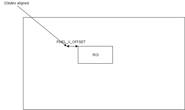
CDMA.PIXEL_X/Y_OFFSET: Configuration of those 2 registers is depending on PIXEL_MAPPING:
PITCH_LINEAR: The address configured to D_DAIN_ADDR_HIGH/LOW_0 should be 32bytes aligned, however, the start address of an ROI might not aligned to that address. Then, PIXEL_X_OFFSET is introduced.
D_DAIN_ADDR_HIGH/LOW_0 = roi_address &(~0x1F); // The nearest 32bytes aligned address; PIXEL_X_OFFSET=(roi_address&0x1F)/bytes_per_pixel // The offset in unit of pixel PIXEL_Y_OFFSET = 0; // The 32bytes aligned address and roi address should be in the same line |
CSC.WEIGHT/DATAIN_SIZE_EXT: The input weight/feature cube size seen from CSC. SW should configure those values based on formula below:
DATAIN_SIZE_EXT: (W/H/C is the width/height/channel of input data cube)
Mode |
Width |
Height |
Channel |
|---|---|---|---|
Winograd |
ceil((W+(PL+PR) )/stride_x) |
ceil((H+PT+PB)/ stride_y) |
C*stride_x*stri de_y |
Image input |
W |
H |
C |
Direct |
W |
H |
C |
WEIGHT_SIZE_EXT (S/R/C is the width/height/channel of input weight cube and let C’ be 32bytes aligned version of C, which means: C’=ceil(C, 16) for INT/FP16 and C’=ceil(C, 32)):
Mode |
Width |
Height |
Channel |
|---|---|---|---|
Winograd |
4 (The size after pre-transform) |
4 (The size after pre-transform) |
C’*stride_x*str ide_y |
Image input |
1 |
R |
C*S |
Direct_CONV |
S |
R |
C |
CSC.CONV_STRIDE_X/Y_EXT: The stride size seen from CSC. (SX/SY is the stride size configured for CDMA: D_CONV_STRIDE)
Mode |
Stride_X |
Stride_Y |
|---|---|---|
Winograd |
1 |
1 |
Image input |
SX |
SY |
Direct_CONV |
SX |
SY |
CSC.D_ATOMICS: Hardware uses this register to decide stripe size:
int calc_stripe_size(int atomics, int processed)
{
    int stripe_size;
    int remain_atomics = atomics - processed;
    if ( remain_atomics < 32 && remain_atomics >= 16 ) {
        stripe_size = remain_atomics;
    } else {
        assert(remain_atomics > 16);
        stripe_size = 16;
    }

    return stripe_size;
}
The register value of D_ATOMICS itself is calculated by:
int calc_atomics(int out_width, int out_height)
{
    return out_width*out_height-1;
}
CSC.D_RELEASE: Hardware uses this field to decide how many input slices should be released after current hardware layer.
<CDMA|CSC>.ZERO_PADDING_VALUE: see Convolution convertors. Be noticed both CDMA and CSC has this register, but they has different meaning:
For CDMA, the padding value in register will be operated w/ CDMA input convertor, the convert output is the actual padding value applied;
For CSC, the padding value in register will be directly applied w/o any more operation;
CACC.D_DATAOUT_MAP:
This register is used to control the data reordering logic in CACC, the configuration of this register should follow the table below:
Configure |
Line_Packed |
Surf_Packed |
|---|---|---|
1x1 |
True |
True |
Multi-Batch mode |
False |
False |
Direct convolution |
False |
False |
Winograd |
False |
False |
CACC. D_DATAOUT_SIZE_0
This register is used to set the output size of convolution:
CONV_MODE |
DATAOUT_WIDTH |
DATAOUT_HEIGHT |
|---|---|---|
DC |
S’=(S-1)*dilation_x + 1 (LP+RP-S’)/stride_x + 1 |
R’=(R-1)*dilation_y + 1 (TP+H+BP-R’)/stride_y + 1 |
IMG |
(LP+W+RP-S)/stride_x + 1 |
(TP+H+BP-R)/stride_y + 1 |
Winograd |
CSC.WIDTH_EXT – 4 |
CSC.HEIGHT_EXT - 4 |
Deconvolution
Deconvolution is a software feature, but it’s necessary to mention the basic flow here to help user understand how it’s supported.
There’re 2 phases:
Convolution:
This phase includes conv_stride_x * conv_stride_y hardware layers.
Software should split the kernels to conv_stride_x*conv_stride_y sets. Suppose the original kernel size is: RxSxC, the splitted kernel size is:
S’=ceil(S/stride_x)
R’=ceil(R/stride_y)
C’=C
K’=K
Kick-off convolution hardware layers based on different kernel set. The output cube size of each hardware layer is:
W’ = (W-S’)+1
H’=(H-R’)+1
C’=K
Reorder:
The output cube from phase I is not the order we want, Rubik engine should be employed to reorder it.
There’re 2 options about how those hardware layers should be scheduled:
Finish all stride_x*stride_y hardware layers then start rubik, total hardware layers is: stride_x*stride_y (convolution) + 1 (rubik);
Finish stride_x convolution hardware layers then start rubik, total hardware layers is: (stride_x + 1)*stride_y;
Generally, b) is the suggested scheduling strategy because:
It has better performance, here’s a timeline diagram which shows method a) vs b). It shows b) is (stride_x*stride_y-1)*t1 quicker than a).

Method b) has smaller memory footprint requirement (W’, H’ are the output width/height of each convolution hardware layer).
Method |
Convolution output buffer |
Rubik output buffer |
Total |
|---|---|---|---|
Method a) |
W’*H’*K*stride_ x*stride_y |
W’*H’*K*stride_ x*stride_y |
2*W’*H’*K*strid e_x*stride_y |
Method b) |
W’*H’*K*stride_ x*2 (x2 is not mandatory but suggested for performance) |
W’*H’*K*stride_ x*stride_y |
W’*H’*K*stride_ x*(stride_y+2) |
For most case, stride_y>2 thus method b) has smaller memory requirement.
SDP programming
Not all the use scenarios in Table 51 are necessary to explain, we’ll discuss bias addition/batch-norm/element-wise operations below (other features are precision related which already covered by Precision Preservation):
Bias addition
As mentioned in Table 51, bias addition can be done by any of SDP sub-module, let’s take using X1 sub-module for bias addition as an example to explain the programming sequence:
Software has to prepare bias data cube, it has to be INT16 for INT8/16 pipeline and FP16 for FP16 pipeline.
Configure the SDP RDMA (most of the registers are intuitional, will highlights bias specific registers only ):
We use bias addition, so, BRDMA_DATA_USE=ALU should be configured
BRDMA_DATA_MODE configuration is based on bias mode
Configure the SDP BS sub-module:
D_DP_BS_CFG
BS_BYPASS=NO
BS_ALU_BYPASS=NO
BS_ALU_ALGO = SUM
BS_MUL_BYPASS = YES
D_DP_BS_ALU_CFG
For per-element/kernel bias, operands should come from MC:
BS_ALU_SRC = MEM
For per cube bias, operands should come from register:
BS_ALU_SRC = REG
BS_ALU_SRC_VALUE = ?? (The value you want)
BS_ALU_SHIFT_VALUE: Based on precision study results
Batch normalization
Batch normalization can be realized by any of X/Y, let’s still use X1 sub-module as an example to show the steps to program batch normalization:
Software has to tightly pack mean/variance into one data cube (M0V0M1V1…), if mean/variance are 2 bytes per element there’ll be 4 bytes for a mean/variance pair. Those 2 bytes will be interpreted as INT16 for INT8/16 pipe and FP16 for FP16 pipe.
Configure the SDP RDMA (most of the registers are intuitional, will highlights batch-norm specific registers only ):
Both ALU/MUL will be used for batch normalization, so, BRDMA_DATA_USE=BOTH should be configured
BRDMA_DATA_MODE configuration is based on batch normalization mode
Configure the SDP BS sub-module:
D_DP_BS_CFG
BS_BYPASS=NO
BS_ALU_BYPASS=NO
BS_ALU_ALGO = SUM
BS_MUL_BYPASS = NO
D_DP_BS_ALU_CFG
BS_ALU_SRC = MEM (Bias data always from MC regardless of per-kernel/element)
BS_ALU_SHIFT_VALUE: Based on precision study results
D_DP_BS_MUL_CFG
BS_MUL_SRC=MEM
BS_MUL_SHIFT_VALUE: Based on precision study results
For any case when both MUL/ALU are used, we can support combinations below:
ALU |
MUL |
|---|---|
REG |
MC |
MC |
REG |
MC, Per-channel |
MC, Per-channel |
MC, Per-element |
MC, Per-element |
REG |
REG |
Element-wise
Element-wise can be realized by any of SDP sub-unit, again, let’s still use X1 module as an example about the element-wise configuration steps:
Different from bias/batch-norm, the element-wise input cube is from upstream hardware layer thus software didn’t need do anything to prepare surface
Configure the SDP RDMA (most of the registers are intuitional, will highlights element-wise specific registers only ):
BRDMA_DATA_USE=? Is based on element-wise type. For PROD eltwise operation, it should be MUL, otherwise, use ALU;
BRDMA_DATA_MODE= PER_ELEMENT
Configure the SDP BS sub-module:
D_DP_BS_CFG
BS_BYPASS=NO
BS_ALU_BYPASS=? (For eltwise=MAX/SUM)
BS_ALU_ALGO : Based on element-wise operation type
BS_MUL_BYPASS = ? (No, For eltwise=PROD)
D_DP_BS_ALU_CFG
BS_ALU_SRC = MEM
BS_ALU_SHIFT_VALUE: Based on precision study results
D_DP_BS_MUL_CFG
BS_MUL_SRC = MEM
BS_MUL_SHIFT_VALUE: Based on precision study results
Compare mode
Normal comparision
SDP implemented compare mode in Y module to support software based redundant computing.
Use scenarios |
Description |
|---|---|
Offline vs offline |
Both of the 2 data stream are come from MC/SRAM The is used to support postprocessor modules (CDP/PDP) redundant computing |
In this mode, SW will schedule 3 HWLs:
1st HWL to run any module then output result to addr0;
2nd HWL to run exact the same setting as 1st layer then output to addr1;
3rd HWL to run SDP_Y in compare mode which has configuration as:
D_SRC_BASE_ADDR_LOW/HIGH = addr0
D_EW_BASE_ADDR_LOW/HIGH = addr1
D_DP_BS_CFG.BS_BYPASS=YES
D_DP_BN_CFG.BN_BYPASS=YES
D_DP_EW_CFG. EW_BYPASS = NO
D_DP_EW_CFG. EW_ALU_BYPASS=NO
D_DP_EW_CFG. EW_ALU_ALGO=EQL
After 3rd HWL execution done, SW should check D_STATUS to see whether difference found.
NOTE: When SDP EQL mode is enabled, D_FEATURE_MODE_CFG.WINOGAD has to be OFF and D_FEATURE_MODE_CFG.BATCH_NUMBER has to be 0
Batch mode comparison
Batch mode is a special case of offline/offline comparison, as SDP_Y RDMA doesn’t support load multiple data cubes in one HWL, batch mode has to be handled in a special way. There’re 2 cases: In order to facilitate further discussion, we denote symbols below:
Dimension: WxHxC
Batch_Num: N
Batch stride: BATCH_STRIDE
There’re 2 cases depending on the attributes of each data cube:
If the data cube are line packed and surface packed:
For thise case, we’ll treat N data cubes as one super cube:
W’= ceil(C/KPG)*W*H, KPG= is_int8 ? 32:16;
H’=N
C’=KPG
line_stride: BATCH_STRIDE
surface_stride: BATCH_STRIDE*N
Otherwise:
As there’re bubbles between each data cube and the contents of those bubbles are un-determistic, we have to compare those cube one by one thus N HWL are necessary.
PDP programming
The most complex logic for PDP programming is deciding which working mode can be used. PDP supports 3 different working modes:
Mode |
Attribute |
|---|---|
On-the-fly |
Input data comes from SDP, recommended whenever possible |
Offline - No split width |
Comparing with on-the-fly, this mode need one SDP write and one PDP read, this increased the memory traffic |
Offline – split width |
Comparing with “no split width”, this mode need over-fetch between overlapped region thus bandwidth further increased |
The working mode selection strategy is:
As mentioned in Section “Planar Data Processor” of Unit Description document, PDP has 7KB internal buffer to save intermediate results during pooling, thus the maximum supported output width is a fixed number. (Refer to: 10.1.4: calculate_pdp_max_width)
Calculate the actual pooling output:
pooled_width = static_cast<int>(ceil(static_cast<float>(width + pad_left + pad_right - kernel_w) / stride_w)) + 1;
if ((pooled_width - 1) * stride_w >= width + pad_left) {
    --pooled_width;
}
Decide working mode
typedef enum {
    PDP_FLYING_MODE,
    PDP_OFFLINE_MODE,
} pdp_mode;
static pdp_mode get_pdp_mode( int width_output, int max_fly_width, bool is_full_conv )
{
    // convolution mode should also be taking into consideration: If software split
    // convolution layer into different hardware layers, PDP can't working on-the-fly
    return (width_output <= max_fly_width) && is_full_conv ? PDP_FLYING_MODE : PDP_OFFLINE_MODE;
}
If PDP working offline mode, we need to calculate splitted width and split number as well (please see: 10.1.4 for detail)
Be noticed: The pseudo code in: 10.1.3 just configured to make hardware work, if possible, software should try to make sure the starting address (in/out or both) of each splitted band be 256 align, this will greatly improve NVDLA memory throughput.
On-the-fly processing
The programming sequence for on-the-fly PDP mode is (most of the registers are intuitional, will highlights on-the-fly mode specific registers only):
PDP-RDMA is not necessary to config because our input is from SDP;
D_OPERATION_MODE_CFG
POOLING_METHOD: Based on pooling method used in algorithm
FLYING_MODE= ON_FLYING
SPLIT_NUM=0
Offline processing without split width
The programming sequence for this mode is:
Appropriate address/memory type should be set to PDP-RDMA;
D_OPERATION_MODE_CFG
POOLING_METHOD: Based on pooling method used in algorithm
FLYING_MODE= OFF_FLYING
SPLIT_NUM=0
D_PARTIAL_WIDTH_IN
PARTIAL_WIDTH_IN_FIRST=info->first_in_width
D_PARTIAL_WIDTH_OUT
PARTIAL_WIDTH_OUT_FIRST=info->first_out_width
Offline processing with split width
The programming sequence for this mode is:
Appropriate address/memory type should be set to PDP-RDMA;
D_OPERATION_MODE_CFG
POOLING_METHOD: Based on pooling method used in algorithm
FLYING_MODE= OFF_FLYING
SPLIT_NUM=info->split_num
D_PARTIAL_WIDTH_IN
PARTIAL_WIDTH_IN_FIRST=info->first_in_width
PARTIAL_WIDTH_IN_MID=info->split_num==1 ? 0:info->mid_in_width
PARTIAL_WIDTH_IN_LAST= info->last_in_width
D_PARTIAL_WIDTH_OUT
PARTIAL_WIDTH_OUT_FIRST=info->first_out_width
PARTIAL_WIDTH_OUT_MID= info->split_num==1 ? 0:info->mid_out_width
PARTIAL_WIDTH_OUT_LAST= info->last_out_width
When hardware processing done, there’ll be interrupt fired from PDP submodule to inform CPU that PDP hardware layer is done for any of above mode.
Register definition
Beside working modes, it’s also necessary to mention some of the interested registers:
D_POOLING_PADDING_CFG: The padding size on left/right/top/bottom. If greater than 0, D_POOLING_PADDING_VALUE_*_CFG will be appended to input data. This register will be take into account for AVE/MAX/MIN mode;
D_POOLING_PADDING_VALUE_*_CFG: The padded value. This register will be took into account for AVE mode only;
CDP programming
CDP always working on offline, there’s no special mode for CDP and the precision related configuration already discussed. So, skip the CDP programming here.
After hardware layer processing done, there’ll be interrupt fired to CPU.
Debug features
NVDLA implemented debug registers to facilitate silicon debug. Those registers are dedicated per register group and won’t be cleared until the corresponding group starts. It will be incremented by 1 when certain condition meets.
Those registers can be classified as 2 groups below:
Precision debug
If saturation counter (see Convertor statistics) exceed threshold (defined by software), this means convertor parameters (scaling, offset) are in-properly set;
If LUT overflow/underflow counter (LUT Statistics) exceed threshold (defined by software), this means LUT is in-properly set;
Performance debug
NVDLA is a fix function engine, the latency is predictable inside each sub-unit, but the read/write response from out-side is not deterministic thus we implemented performance registers below to help SW analysis the bottleneck of un-expected performance drop.
Sub unit |
Register name |
Description |
|---|---|---|
CDMA |
D_PERF_ENABLE |
Control register to enable/disable perf Counter |
D_PERF_DAT_READ_STAL L |
Count stall cycles of data read DMA for one layer |
|
D_PERF_WT_READ_STALL |
Count total latency of data read DMA for one layer |
|
D_PERF_DAT_READ_LATE NCY |
Count stall cycles of weight read DMA for one layer |
|
D_PERF_WT_READ_LATEN CY |
Count total latency of weight read DMA for one layer |
|
SDP |
D_PERF_ENABLE |
Control register to enable/disable perf Counter |
D_PERF_MRDMA_READ_ST ALL |
Count stall cycles of M read DMA for one layer |
|
D_PERF_BRDMA_READ_ST ALL |
Count stall cycles of B read DMA for one layer |
|
D_PERF_NRDMA_READ_ST ALL |
Count stall cycles of N read DMA for one layer |
|
D_PERF_ERDMA_READ_ST ALL |
Count stall cycles of E read DMA for one layer |
|
D_PERF_WDMA_WRITE_ST ALL |
Count stall cycles of write DMA for one layer |
|
CDP |
D_PERF_ENABLE |
Control register to enable/disable perf Counter |
D_PERF_READ_STALL |
Count stall cycles of read DMA for one layer |
|
D_PERF_WRITE_STALL |
Count stall cycles of wirte DMA for one layer |
|
PDP |
D_PERF_ENABLE |
Control register to enable/disable perf Counter |
D_PERF_READ_STALL |
Count stall cycles of read DMA for one layer |
|
D_PERF_WRITE_STALL |
Count stall cycles of wirte DMA for one layer |
|
RUBIK |
D_PERF_ENABLE |
Control register to enable/disable perf Counter |
D_PERF_READ_STALL |
Count stall cycles of read DMA for one layer |
|
D_PERF_WRITE_STALL |
Count stall cycles of wirte DMA for one layer |
|
BDMA |
CFG_STATUS_PERF_STAL L_COUNT_EN |
Control register to enable/disable perf Counter |
STATUS_PERF_GRP0_REA D_STALL |
Count stall cycles of read DMA for group0 |
|
STATUS_PERF_GRP0_WRI TE_STALL |
Count stall cycles of wirte DMA for group0 |
|
STATUS_PERF_GRP1_REA D_STALL |
Count stall cycles of read DMA for group1 |
|
STATUS_PERF_GRP1_WRI TE_STALL |
Count stall cycles of read DMA for group1 |
For each sub-unit, we have “EN” register to allow software enable/disable those counting register to save power.
Limitation
Though we’ve already highlight hardware restrictions in the chapters above, but we’d like to centralize the limitations here to facilitate users quick check illegal settings.
Data Format
The alignment for address/line_stride/surf_stride in :Table 35 should be satisfied when allocating buffer;
LINE_STRIDE: line stide has to bigger than the actual size per line, please refer to: 10.1.1 for minimal line_stride calculation;
For 1x1xC cube, it should always be line_packed and surf_packed.
CSB_MASTER
Any read access or write access to reserved register address (0x14000~0x3FFFF) is forbidden. CSB master do not support for these addresses. Any access to these addresses may cause unknow result.
BDMA
When both group0 and group1 are both busy, no more command is allowed even if there are free slot
All operations in one BDMA HWL should has the same destination memory type (DST_RAM_TYPE)
Convolution
General
There’re multiple pipeline stages in convolution pipeline, the op_enable programming sequence has to be in reverse order, e.g.: CONV_ACCUCONV_MACCONV_SCCONV_BUFCONV_DMA
WMB and weight data MUST has the same RAM type.
If weight_format=compressed, banks_for_data+banks_for_weight must be less than 16 (Bank 15 is reserved for WMB).
WEIGHT_BANK should be allocated large enough to store one kernel group weight plus 128Bytes; For compression mode, BANK for WMB is fixed as 1, this means WMB for one kernel group should always less than 32KB-128B so that additional 128Bytes can be stored in that bank.
CSC:: RLS_SLICES: This register should never exceed DATAIN_HEIGHT_EXT, Even with the partial release in pervious layer, the unreleased slices will be counted into datain_height_ext of CSC register (but not in datain_height of CDMA register).
For example, in first layer we input 10 slices and release 6 slices, there are 4 slices remain in CBUF.
And with second layer we fetch new 7 slices from CDMA and combined with remain slices to do convolution. The setting of CDMA datain_height should be 7 and CSC datain_height_ext should be (7+4) = 11. And at this time rls_slices should not more than 11.
The right/bottom padding should be carefully configured to make sure all the data will be used for convolution, which means:
Where, PL/PT are the left/top padding which are get from network definition; PR/PB are the right/bottom padding which are configured by user;
Data re-use can be take effect when all conditions below are meet:
Skip_rls is set as true for previous layer;
Conv_mode and DATA_BANK are kept unchanged comparing with previous layer;
Left/Right padding should be less than S, Top/Bottom padding should be less than R
Image
For image input, pixel_y_offset should be set as 0 for pitch linear;
If channel post extension enabled, the limitations in Table 46 has to be meet;
Dilation is not supported
DC
No special limitation;
Winograd
Output width and height must be 4 divisible and >= 8;
The equivalent kernel size should be 3x3;
Multi-batch
The start address of each input feature cube has to be carefully arranged to make sure their offset is a fixed number as BATCH_STRIDE.
Supported feature crossing:
Channel -post extensi on |
Multi-b atch |
Deconv |
Image Input |
Dilatio n |
Winogra d |
|
|---|---|---|---|---|---|---|
Channel -post extensi on |
N |
N |
Y |
N |
N |
|
Multi-b atch |
N |
Y |
N |
Y |
N |
|
Deconv |
N |
Y |
N |
N |
N |
|
Image In |
Y |
N |
N |
N |
N |
|
Dilatio n |
N |
Y |
N |
N |
N |
|
Winogra d |
N |
N |
N |
N |
N |
LUT
For linear mode, the table start/end should meet the requirements below:
LE_END-LE_START == 1<<(LE_INDEX_SELECT+6)
LO_END-LO_START == 1<<(LO_INDEX_SELECT+8)
For linear mode, the “select” field shouldn’t exceed the bit-depth of hardware thus we have limitations below:
SDP |
CDP |
|
|---|---|---|
INT8 |
LE: [-6~25] LO: [-8~23] |
LE: [-6~15] LO: [-8~13] |
INT16 |
LE: [-6~25] LO: [-8~23] |
LE: [-6~31] LO: [-8~29] |
FP16 |
LO: [-128, 119] LE: [-128, 121] |
LO: [-128, 119] LE: [-128, 121] |
For FP16 above, another constrain should take into consideration: LX_START/END registers are FP32 and:
LE_END = LE_START + pow(2, LE_INDEX_SELECT +6)
In order to make sure LE_END larger than LE_START, constrain below should be satisfied:
LE_START/pow(2, LE_INDEX_SELECT +6) < pow(2, 24), thus:
LE_START < pow(2, LE_INDEX_SELECT+30)
For the same reason, LO_START < pow(2, LO_INDEX_SELECT+32)
For exponential mode, the table start/end should meet the requirements below:
LE_END-LE_START==(1<<(LE_INDEX_OFFSET+64)).
If the value calculated by formula below exceed the INT32/FP32 representable, use INT32_MAX or FP32_MAX instead.
For exponential mode, we also have constrain on LE_INDEX_OFFSET:
SDP |
CDP |
|
|---|---|---|
INT8 |
[-64, 31] |
[-64, 20] |
INT16 |
[-64, 31] |
[-64, 36] |
FP16 |
[-126, 127] |
[-126, 127] |
SDP
General
When SRC is configured as REG, corresponding RDMA shouldn’t be enabled.
If EQL mode is enabled, Y ALU convertor must be bypassed (except FP16) and all the operations after ALU should be bypassed.
If PReLU is enabled for one sub-unit, the ALU in that unit MUST be bypassed.
For PROC_PRECISION==FP16:
If EW_ALU_BYPASS==NO && D_DP_EW_ALU_CFG. EW_ALU_SRC==MEM, then, EW_ALU_CVT_BYPASS must be NO;
If EW_MUL_BYPASS==NO && D_DP_EW_MUL_CFG. EW_MUL_SRC==MEM, then, EW_MUL_CVT_BYPASS must be NO;
DC
Precision conversion is not allowed if SDP output to PDP or EQL mode;
For INT16INT8, HW has no requirement on channel size configuration, but if C is not 32 elements aligned, HW will read/write the additional memory thus SW has to guarantee the allocated src/dst data cube is big enough;
Winograd/Batch
SDP has to work on the fly with CC
SDP_Y can’t work at EQL mode (EW_ALU_ALGO != EQL)
If multi-batch is enabled, registers below has to be 64 bytes aligned:
DST_BASE_ADDRDST_LINE_STRIDEDST_SURFACE_STRIDEBS/BN/EW_BS_BASE_ADDR_LOW/HIGH
CDP
Maximum supported local_size is 9.
PDP
PL/PR should be carefully programmed to make sure each input sample are used:
(PL+W+PR-Kernel_W)%stride_x == 0
PL/PR should be less than kernel_width;
For any mode, first/mid/last_out_width should be less than maximum flying width (see 10.1.4)
For non-split mode, CUBE_IN_WIDTH + PL should be equals to (CUBE_OUT_WIDTH-1)*stride_x + kernel_width;
For split mode:
For split_num =2:
First_out_width + last_out_width should be equals to CUBE_OUT_WIDTH;
First_in_width + PL should be equals to (first_out_width-1)*stride_x + kernel_width;
Last_in_width + PR + overlap should be equals to (last_out_width-1)*stride_x + kernel_width;
if kernel >=kernel_stride, kernel_w – stride_x should be <= first_in_width; Otherwise, stride_x – kernel_w < last_in_width;
For split_num > 2:
first_out_width + last_out_width + mid_out_width*(split_num-2) should be equals to CUBE_OUT_WIDTH;
first_in_width + PL should be equals to (first_out_width-1)*stride_x + kernel_w;
mid_in_width + overlap should be equals to (mid_out_width-1)*stride_x + kernel_w;
last_in_width + PR + overlap should be equals to (last_out_width-1)*stride_x + kernel_w;
if kernel_w >=kernel_stride, kernel_w – stride_x should be <= <first|mid>_in_width; Otherwise, stride_x – kernel_w should be < <last|mid>_in_width;
Maximum supported pooling kernel size is 8
Rubik
For contract mode, the address/line_stride for both input/output should be 32bytes aligned;
For split/merge mode, the address/line_stride should be 64bytes aligned for planar data(output of split mode, input of merge mode)
deconv_x_stride * datain_width should be <=8192