Scalability parameters and ConfigROM
Scalability parameters
Note that the current source code has only been tested for the nv_small configuration, and while the nv_small configuration passes many tests, additionall coverage is necessary to get it to tapeout quality.
Scalability Parameter |
Description |
INT8 Large Config(nv_large ) |
INT8 Small Config(nv_small ) |
|---|---|---|---|
NVDLA_FEATURE_D ATA_TYPE_BINARY /INT4/INT8/INT16 INT32/FP16/FP32 /FP64 |
Identify the data type of input feature data |
INT8 |
INT8 |
NVDLA_WEIGHT_D ATA_TYPE_BINARY /INT4/INT8/INT16 INT32/FP16/FP32 /FP64 |
Identify the data type of input weight data |
INT8 |
INT8 |
NVDLA_WEIGHT_CO MPRESSION_ENABL E |
Support of the feature of weight compression. Disable this can save area in CBUF |
YES |
NO |
NVDLA_WINOG RAD_ENABLE |
Support of the optimization feature of weight compression. Disable this can save area of CSC/CMAC/CACC |
YES |
NO |
NVDLA_MAC_ATOMI C_C_SIZE |
MAC atomic size of input channel number |
64 |
8 |
NVDLA_MAC_ATOMI C_K_SIZE |
MAC atomic size of output kernel number |
32 |
8 |
NVDLA_MEMORY_A TOMIC_SIZE |
Memory smallest access size, also the data cube is aligned with this size. Note: the size is # of feature data type |
32 |
8 |
NVDLA_BATCH_ENA BLE |
Support of optimization feature of batch. Disable this can save area in SDP/CACC/CSC/CD MA |
YES |
No |
NVDLA_MAX_BATCH _SIZE |
Maximum batch size, this will directly impact the local buffer size |
32 |
|
NVDLA_CBUF_BANK _NUMBER |
Convolutional buffer bank number |
16 |
32 |
NVDLA_CBUF_BANK _WIDTH |
Convolutional buffer bank data width |
64B |
8B |
NVDLA_CBUF_BANK _DEPTH |
Convolutional buffer bank depth |
512 |
512 |
NVDLA_SECONDARY _MEMIF_ENABLE |
Support the secondary memory interface (SRAMIF) |
Yes |
No |
NVDLA_SDP_LUT_E NABLE |
SDP support Look-up-Table for non-linear function |
Yes |
No |
NVDLA_SDP_BS_E NABLE |
SDP support Bias/Scaling function |
Yes |
Yes |
NVDLA_SDP_BN_E NABLE |
SDP support Batch-Normaliza tion function |
Yes |
Yes |
NVDLA_SDP_EW_E NABLE |
SDP support Element-wise-op eration function |
Yes |
No |
NVDLA_SDP_BS_TH ROUGHPUT |
Throughput of SDP Bias/Scaling function |
16 |
1 |
NVDLA_SDP_BN_TH ROUGHPUT |
Throughput of SDP Batch-Normaliza tion function |
16 |
1 |
NVDLA_SDP_EW_TH ROUGHPUT |
Throughput of SDP Element-wise-op eration function |
4 |
|
NVDLA_BDMA_ENA BLE |
Support the bridge DMA engine function |
Yes |
No |
NVDLA_RUBIK_ENA BLE |
Support the rubik engine function |
Yes |
No |
NVDLA_PDP_ENABL E |
Support PDP engine function |
Yes |
Yes |
NVDLA_PDP_THROU GHPUT |
Throughput of PDP engine function |
8 |
1 |
NVDLA_CDP_ENAB LE |
Support CDP engine function |
Yes |
Yes |
NVDLA_CDP_THROU GHPUT |
Throughput of CDP engine function |
8 |
1 |
NVDLA_PRIMARY_M EMIF_MAX_BURST _LENGTH |
Primary memory interface maximum burst length number |
1 |
4 |
NVDLA_PRIMARY_M EMIF_WIDTH |
Primary memory interface data width |
64B |
8B |
NVDLA_PRIMARY_M EMIF_LATENCY |
Primary memory interface data return latency cycles for read access |
1200 |
50 |
NVDLA_SECONDARY _MEMIF_MAX_BURS T_LENGTH |
Secondary memory interface (SRAMIF) maximum burst length number |
4 |
|
NVDLA_SECONDARY _MEMIF_WIDTH |
Secondary memory interface (SRAMIF) data width |
64B |
|
NVDLA_SECONDARY _MEMIF_LATENCY |
Secondary memory interface (SRAMIF) data return latency cycles for read access |
128 |
|
NVDLA_MEMIF_ADD RESS_WIDTH |
Address bit width for external memory interface |
64 |
32 |
More Details
NVDLA_MAC_ATOMIC_C_SIZE and NVDLA_MAC_ATOMIC_K_SIZE
These two parameters affect determine the number of mac cells and number of multipliers in each mac cell. The total number of multipliers is NVDLA_MAC_ATOMI C_C_SIZE * NVDLA_MAC_ATOMI C_K_SIZE. The number of kernels in one kernel group is NVDLA_MAC_ATOMI C_K_SIZE.
NVDLA_MEMORY_ATOMIC_SIZE
This parameter determines the size of one atomic cube which is 1x1xNVDLA_MEMORY_ATOMIC_SIZE. Feature, Weight, Bias, PReLU, Batch Normalization and Element-Wise data cubes are split into atomic cubes before loaded or stored into memory. In nvdlav1 and nv_large configurations, size of atomic cbue is 1x1x32. In nv_small configuration, it’s 1x1x8. Line stride and surface stride should also align to NVDLA_MEMORY_ATOMIC_SIZE.
NVDLA_CBUF_BANK_NUMBER, NVDLA_CBUF_BANK_WIDTH and NVDLA_CBUF_BANK_DEPTH
These parameters determine the size of cbuf. (NVDLA_CBUF_BANK_NUMBER * NVDLA_CBUF_BANK_WIDTH * NVDLA_CBUF_BANK_DEPTH) For nv_small, the size is 32*8*512 = 128KB. For nv_small_256, the size is 32*32*128 = 128KB.
Config nv_small_256
This config is created for higher convolution performance than nv_small. Comparing with nv_small, the difference is that CMAC has 256 multipliers, not 64. In this configuration NVDLA_MAC_ATOMIC_C_SIZE is 32 and NVDLA_MAC_ATOMI C_K_SIZE is 8. Accordingly, NVDLA_CBUF_BANK _WIDTH is 32 and NVDLA_CBUF_BANK _DEPTH is 128.
Sub-unit identifier table
Sub-unit Identifier |
Sub-unit Name |
|---|---|
0x0000 |
End of list |
0x0001 |
GLB |
0x0002 |
CIF |
0x0003 |
CDMA |
0x0004 |
CBUF |
0x0005 |
CSC |
0x0006 |
CMAC |
0x0007 |
CACC |
0x0008 |
SDP_RDMA |
0x0009 |
SDP |
0x000a |
PDP_RDMA |
0x000b |
PDP |
0x000c |
CDP_RDMA |
0x000d |
CDP |
0x000e |
BDMA |
0x000f |
RUBIK |
Note:
CIF(ID=0x0002) can be configured to MCIF or SRAMIF.
There are two CMACs in nv_small and nv_large. (CMAC_A and CMAC_B)
CBUF doesn’t have registers.
Descriptors and payloads of sub-units in ConfigROM
The reg offset in bellow tables are the relative offset to the beginning of current descriptor.
GLB
Reg offset (in Byte) |
Reg name |
Reg fields |
Value in nv_small config |
Value in nv_large config |
|---|---|---|---|---|
0x0 |
GLB_DESC |
Bits 0-15: unit id. Bits 16-31: payload length. |
0x00000001 |
0x00000001 |
CIF
Reg offset (in Byte) |
Reg name |
Reg fields |
Value in nv_smal l config |
Value in nv_larg e config (MCIF) |
Value in nv_larg e config (SRAMIF ) |
|
|---|---|---|---|---|---|---|
0x0 |
CIF_DES C |
Bits 0-15: unit id. Bits 16-31: payload length. |
0x00180 002 |
0x00180 002 |
0x00180 002 |
|
Incompa tible capabil ities |
0x4 |
CIF_CAP _INCOMP AT |
0x0 |
0x0 |
0x0 |
|
Compati ble capabil ities |
0x8 |
CIF_CAP _COMPAT |
bit 0: CIF_IS _SRAM. Set to 1 if this CIF is connect ed to a separat e SRAM block. |
0x0 |
0x0 |
0x1 |
Baselin e paramet ers |
0xc |
CIF_BAS E_WIDTH |
bits 0-7: width (max 256B) |
0x8 |
0x40 |
0x40 |
0x10 |
CIF_BAS E_LATEN CY |
bits 0-15: latency (max 65535 cycles) |
0x32 |
0x4b0 |
0x80 |
|
0x14 |
CIF_BAS E_ BURST_L ENGTH_M AX |
bits 0-7: max_bur st_leng th (max 256B) |
0x4 |
0x4 |
0x4 |
|
0x18 |
CIF_BAS E_MEM_A DDR_WID TH |
memory interfa ce address width |
0x20 |
0x40 |
0x40 |
CDMA
Reg offset (in Byte) |
Reg name |
Reg fields |
Value in nv_small config |
Value in nv_large config |
|
|---|---|---|---|---|---|
0x0 |
CDMA_DES C |
Bits 0-15: unit id. Bits 16-31: payload length. |
0x003400 03 |
0x003400 03 |
|
Incompat ible capabili ties |
0x4 |
CDMA_CAP _INCOMPA T |
0x0 |
0x0 |
|
Compatib le capabili ties |
0x8 |
CDMA_CAP _COMPAT |
bit 0: WINOGRAD bit 1: MULTI_BA TCH bit 2: FEATURE_ COMPRESS ION bit 3: WEIGHT_C OMPRESSI ON bit 4: IMAGE_IN bit 31: 1’b0 |
0x10 |
0x1b |
Baseline paramete rs |
0xc |
CDMA_BAS E_FEATUR E_TYPES |
Supporte d data types of input feature data |
0x10 |
0x10 |
0x10 |
CDMA_BAS E_WEIGHT _TYPES |
Supporte d data types of input weight data |
0x10 |
0x10 |
|
0x14 |
CDMA_BAS E_ATOMIC _C |
atomic_c |
0x8 |
0x40 |
|
0x18 |
CDMA_BAS E_ATOMIC _K |
atomic_k |
0x8 |
0x20 |
|
0x1c |
CDMA_BAS E_ATOMIC _M |
atomic_m |
0x8 |
0x20 |
|
0x20 |
CDMA_BAS E_CBUF_B ANK_NUM |
cbuf_ban k_number |
0x20 |
0x10 |
|
0x24 |
CDMA_BAS E_CBUF_B ANK_WIDT H |
cbuf_ban k_width |
0x8 |
0x40 |
|
0x28 |
CDMA_BAS E_CBUF_B ANK_DEPT H |
cbuf_ban k_depth |
0x200 |
0x200 |
|
Capabili ties’ paramete rs |
0x2c |
CDMA_MUL TI_BATCH _MAX |
max_batc h |
0x0 |
0x20 |
0x30 |
CDMA_IMA GE_IN_FO RMATS_PA CKED |
Supporte d packed image formats |
0x0cfff0 01 |
0x0cfff0 01 |
|
0x34 |
CDMA_IMA GE_IN_FO RMATS_SE MI |
Supporte d semi-pla nar image formats |
0x3 |
0x3 |
CBUF
Reg offset (in Byte) |
Reg name |
Reg fields |
Value in nv_small config |
Value in nv_large config |
|
|---|---|---|---|---|---|
0x0 |
CBUF_DES C |
Bits 0-15: unit id. Bits 16-31: payload length. |
0x001800 04 |
0x001800 04 |
|
Incompat ible capabili ties |
0x4 |
CBUF_CAP _INCOMPA T |
0x0 |
0x0 |
|
Compatib le capabili ties |
0x8 |
CBUF_CAP _COMPAT |
0x0 |
0x0 |
|
Baseline paramete rs |
0xc |
CBUF_BAS E_BANK_N UM |
cbuf_ban k_number |
0x20 |
0x10 |
0x10 |
CBUF_BAS E_BANK_W IDTH |
cbuf_ban k_width |
0x8 |
0x40 |
|
0x14 |
CBUF_BAS E_BANK_D EPTH |
cbuf_ban k_depth |
0x200 |
0x200 |
|
0x18 |
CBUF_BAS E_CDMA_I D |
cdma_id |
0x3 |
0x4 |
CSC
Reg offset (in Byte) |
Reg name |
Reg fields |
Value in nv_small config |
Value in nv_large config |
|
|---|---|---|---|---|---|
0x0 |
CSC_DESC |
Bits 0-15: unit id. Bits 16-31: payload length. |
0x003000 05 |
0x003000 05 |
|
Incompat ible capabili ties |
0x4 |
CSC_CAP_ INCOMPAT |
0x0 |
0x0 |
|
Compatib le capabili ties |
0x8 |
CSC_CAP_ COMPAT |
bit 0: WINOGRAD bit 1: MULTI_BA TCH bit 2: FEATURE_ COMPRESS ION bit 3: WEIGHT_C OMPRESSI ON bit 4: IMAGE_IN bit 31: 1’b0 |
0x10 |
0x1b |
Baseline paramete rs |
0xc |
CSC_BASE _FEATURE _TYPES |
Supporte d data types of input feature data |
0x10 |
0x10 |
0x10 |
CSC_BASE _WEIGHT_ TYPES |
Supporte d data types of input weight data |
0x10 |
0x10 |
|
0x14 |
CSC_BASE _ATOMIC_ C |
atomic_c |
0x8 |
0x40 |
|
0x18 |
CSC_BASE _ATOMIC_ K |
atomic_k |
0x8 |
0x20 |
|
0x1c |
CSC_BASE _ATOMIC_ M |
atomic_m |
0x8 |
0x20 |
|
0x20 |
CSC_BASE _CBUF_BA NK_NUM |
cbuf_ban k_number |
0x20 |
0x10 |
|
0x24 |
CSC_BASE _CBUF_BA NK_WIDTH |
cbuf_ban k_width |
0x8 |
0x40 |
|
0x28 |
CSC_BASE _CBUF_BA NK_DEPGT H |
cbuf_ban k_depth |
0x200 |
0x200 |
|
0x2c |
CSC_BASE _CDMA_ID |
cdma_id |
0x3 |
0x4 |
|
Capabili ties’ paramete rs |
0x30 |
CSC_MULT I_BATCH_ MAX |
max_batc h |
0x0 |
0x20 |
CMAC
There are two CMAC (CMAC_A and CMAC_B) in NVDLA nv_small and nv_large design. Their descriptors and payloads are same. They use different slots of address space.
Reg offset (in Byte) |
Reg name |
Reg fields |
Value in nv_small config |
Value in nv_large config |
|
|---|---|---|---|---|---|
0x0 |
CMAC_DES C |
Bits 0-15: unit id. Bits 16-31: payload length. |
0x001c00 06 |
0x001c00 06 |
|
Incompat ible capabili ties |
0x4 |
CMAC_CAP _INCOMPA T |
0x0 |
0x0 |
|
Compatib le capabili ties |
0x8 |
CMAC_CAP _COMPAT |
bit 0: WINOGRAD bit 31: 1’b0 |
0x0 |
0x0 |
Baseline paramete rs |
0xc |
CMAC_BAS E_FEATUR E_TYPES |
Supporte d data types of input feature data |
0x10 |
0x10 |
0x14 |
CMAC_BAS E_ATOMIC _C |
atomic_c |
0x8 |
0x40 |
|
0x18 |
CMAC_BAS E_ATOMIC _K |
atomic_k |
0x8 |
0x20 |
|
0x1c |
CMAC_BAS E_CDMA_I D |
cdma_id |
0x3 |
0x4 |
CACC
Reg offset (in Byte) |
Reg name |
Reg fields |
Value in nv_small config |
Value in nv_large config |
|
|---|---|---|---|---|---|
0x0 |
CACC_DES C |
Bits 0-15: unit id. Bits 16-31: payload length. |
0x002000 07 |
0x002000 07 |
|
Incompat ible capabili ties |
0x4 |
CACC_CAP _INCOMPA T |
0x0 |
0x0 |
|
Compatib le capabili ties |
0x8 |
CACC_CAP _COMPAT |
bit 0: WINOGRAD bit 1: MULTI_BA TCH bit 31: 1’b0 |
0x0 |
0x3 |
VBaselin e paramete rs |
0xc |
CACC_BAS E_FEATUR E_TYPES |
Supporte d data types of input feature data |
0x10 |
0x10 |
0x10 |
CACC_BAS E_WEIGHT _TYPES |
Supporte d data types of input weight data |
0x10 |
0x10 |
|
0x14 |
CACC_BAS E_ATOMIC _C |
atomic_k |
0x8 |
0x20 |
|
0x18 |
CACC_BAS E_ATOMIC _K |
atomic_m |
0x8 |
0x20 |
|
0x1c |
CACC_BAS E_CDMA_I D |
cdma_id |
0x3 |
0x4 |
|
Capabili ties’ paramete rs |
0x20 |
CACC_MUL TI_BATCH _MAX |
max_batc h |
0x0 |
0x20 |
SDP_RDMA
Reg offset (in Byte) |
Reg name |
Reg fields |
Value in nv_small config |
Value in nv_large config |
|
|---|---|---|---|---|---|
0x0 |
SDP_RDMA _DESC |
Bits 0-15: unit id. Bits 16-31: payload length. |
0x000e00 08 |
0x000e00 08 |
|
Incompat ible capabili ties |
0x4 |
SDP_RDMA _CAP_INC OMPAT |
0x0 |
0x0 |
|
Compatib le capabili ties |
0x8 |
SDP_RDMA _CAP_COM PAT |
0x0 |
0x0 |
|
Baseline paramete rs |
0xc |
SDP_RDMA _BASE_AT OMIC_M |
atomic_m |
0x8 |
0x20 |
0xe |
SDP_RDMA _BASE_SD P_ID |
sdp_id (slot id of correspo nding sdp) |
0x9 |
0xa |
SDP
Reg offset (in Byte) |
Reg name |
Reg fields |
Value in nv_small config |
Value in nv_large config |
|
|---|---|---|---|---|---|
0x0 |
SDP_DESC |
Bits 0-15: unit id. Bits 16-31: payload length. |
0x002000 09 |
0x002000 09 |
|
Incompat ible capabili ties |
0x4 |
SDP_CAP_ INCOMPAT |
0x0 |
0x0 |
|
Compatib le capabili ties |
0x8 |
SDP_CAP_ COMPAT |
bit 0: WINOGRAD bit 1: MULTI_BA TCH bit 2: LUT bit 3: BS bit 4: BN bit 5: EW bit 31: 1’b0 |
0x18 |
0x3f |
Baseline paramete rs |
0xc |
SDP_BASE _FEATURE _TYPES |
Supporte d data types of input feature data |
0x10 |
0x10 |
0x10 |
SDP_BASE _CDMA_ID |
cdma_id |
0x3 |
0x4 |
|
Capabili ties’ paramete rs |
0x14 |
SDP_MULT I_BATCH_ MAX |
max_batc h |
0x0 |
0x20 |
0x18 |
SDP_ BS_THROU GHPUT |
bs_throu ghput |
0x1 |
0x10 |
|
0x1c |
SDP_ BN_THROU GHPUT |
bn_throu ghput |
0x1 |
0x10 |
|
0x20 |
SDP_ EW_THROU GHPUT |
ew_throu ghput |
0x0 |
0x4 |
PDP_RDMA
Reg offset (in Byte) |
Reg name |
Reg fields |
Value in nv_small config |
Value in nv_large config |
|
|---|---|---|---|---|---|
0x0 |
PDP_ RDMA_DES C |
Bits 0-15: unit id. Bits 16-31: payload length. |
0x000e00 0a |
0x000e00 0a |
|
Incompat ible capabili ties |
0x4 |
PDP_ RDMA_CAP _INCOMPA T |
0x0 |
0x0 |
|
Compatib le capabili ties |
0x8 |
PDP_ RDMA_CAP _COMPAT |
0x0 |
0x0 |
|
Baseline paramete rs |
0xc |
PDP_RDMA _BASE_AT OMIC_M |
atomic_m |
0x8 |
0x20 |
0xe |
PDP_RDMA _BASE_PD P_ID |
pdp_id (slot id of correspo nding pdp) |
0xb |
0xc |
PDP
Reg offset (in Byte) |
Reg name |
Reg fields |
Value in nv_small config |
Value in nv_large config |
|
|---|---|---|---|---|---|
0x0 |
PDP_DESC |
Bits 0-15: unit id. Bits 16-31: payload length. |
0x001000 0b |
0x001000 0b |
|
Incompat ible capabili ties |
0x4 |
PDP_CAP_ INCOMPAT |
0x0 |
0x0 |
|
Compatib le capabili ties |
0x8 |
PDP_CAP_ COMPAT |
0x0 |
0x0 |
|
Baseline paramete rs |
0xc |
PDP_BASE _FEATURE _TYPES |
Supporte d data types of input feature data |
0x10 |
0x10 |
0x10 |
PDP_BASE _THROUGH PUT |
throughp ut |
0x1 |
0x8 |
CDP_RDMA
Reg offset (in Byte) |
Reg name |
Reg fields |
Value in nv_small config |
Value in nv_large config |
|
|---|---|---|---|---|---|
0x0 |
CDP_DESC |
Bits 0-15: unit id. Bits 16-31: payload length. |
0x000e00 0c |
0x000e00 0c |
|
Incompat ible capabili ties |
0x4 |
CDP_ RDMA_CAP _INCOMPA T |
0x0 |
0x0 |
|
Compatib le capabili ties |
0x8 |
CDP_ RDMA_CAP _COMPAT |
0x0 |
0x0 |
|
Baseline paramete rs |
0xc |
CDP_RDMA _BASE_AT OMIC_M |
atomic_m |
0x8 |
0x20 |
0xe |
CDP_RDMA _BASE_PD P_ID |
cdp_id (slot id of correspo nding cdp) |
0xd |
0xe |
CDP
Reg offset (in Byte) |
Reg name |
Reg fields |
Value in nv_small config |
Value in nv_large config |
|
|---|---|---|---|---|---|
0x0 |
CDP_DESC |
Bits 0-15: unit id. Bits 16-31: payload length. |
0x001000 0d |
0x001000 0d |
|
Incompat ible capabili ties |
0x4 |
CDP_CAP_ INCOMPAT |
0x0 |
0x0 |
|
Compatib le capabili ties |
0x8 |
CDP_CAP_ COMPAT |
0x0 |
0x0 |
|
Baseline paramete rs |
0xc |
CDP_BASE _FEATURE _TYPES |
Supporte d data types of input feature data |
0x10 |
0x10 |
0x10 |
CDP_BASE _THROUGH PUT |
throughp ut |
0x1 |
0x8 |
BDMA
Reg offset (in Byte) |
Reg name |
Reg fields |
Value in nv_small config |
Value in nv_large config |
|---|---|---|---|---|
0x0 |
BDMA_DESC |
Bits 0-15: unit id. Bits 16-31: payload length. |
0x0004000e |
0x0004000e |
RUBIK
Reg offset (in Byte) |
Reg name |
Reg fields |
Value in nv_small config |
Value in nv_large config |
|---|---|---|---|---|
0x0 |
RUBIK_DESC |
Bits 0-15: unit id. Bits 16-31: payload length. |
0x0004000f |
0x0004000f |
Supported data types or weight types
Below table lists the fields of registers of supported data types or weight types in above sections
Bit |
Data type or Weight type |
|---|---|
0 |
Binary |
1 |
INT4 |
2 |
UINT4 |
3 |
INT8 |
4 |
UINT8 |
5 |
INT16 |
6 |
UINT16 |
7 |
INT32 |
8 |
UINT32 |
9 |
FP16 |
10 |
FP32 |
11 |
FP64 |
Supported packed image formats
Below table lists the fields of registers of supported packed image formats in above sections
Bit |
Image format |
|---|---|
0 |
R8 |
1 |
R10 |
2 |
R12 |
3 |
R16 |
4 |
R16_I |
5 |
R16_F |
6 |
A16B16G16R16 |
7 |
X16B16G16R16 |
8 |
A16B16G16R16_F |
9 |
A16Y16U16V16 |
10 |
V16U16Y16A16 |
11 |
A16Y16U16V16_F |
12 |
A8B8G8R8 |
13 |
A8R8G8B8 |
14 |
B8G8R8A8 |
15 |
R8G8B8A8 |
16 |
X8B8G8R8 |
17 |
X8R8G8B8 |
18 |
B8G8R8X8 |
19 |
R8G8B8X8 |
20 |
A2B10G10R10 |
21 |
A2R10G10B10 |
22 |
B10G10R10A2 |
23 |
R10G10B10A2 |
24 |
A2Y10U10V10 |
25 |
V10U10Y10A2 |
26 |
A8Y8U8V8 |
27 |
V8U8Y8A8 |
Supported semi-planar image formats
Below table lists the fields of registers of supported semi-planar image formats in above sections
Bit |
Image format |
|---|---|
0 |
Y8___U8V8_N444 |
1 |
Y8___V8U8_N444 |
2 |
Y10___U10V10_N444 |
3 |
Y10___V10U10_N444 |
4 |
Y12___U12V12_N444 |
5 |
Y12___V12U12_N444 |
6 |
Y16___U16V16_N444 |
7 |
Y16___V16U16_N444 |
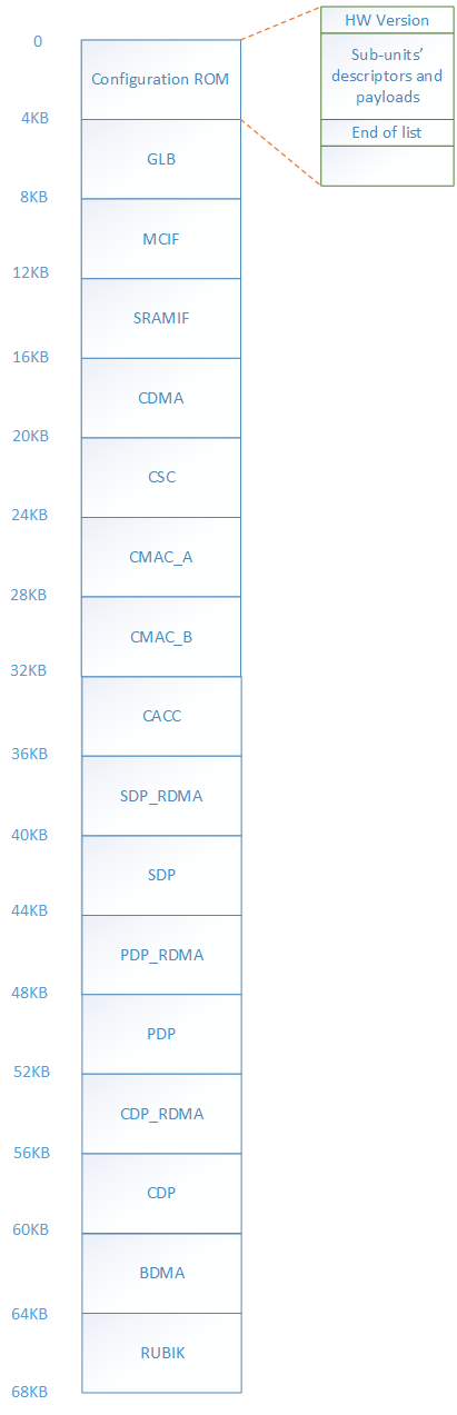
Address space layout
In the address space layout, the order of sub-units is same as the order of the descriptors in Configuration ROM. The size of one slot is 4KB.
nv_small:
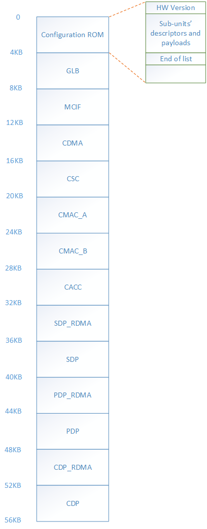
nv_large: