Integrator’s Manual
Introduction
This document introduces essential knowledge for how to integrate NVDLA into an SoC. It includes detail on bus interfaces, power on sequence, address map, cell requirements, and synthesis.
The open source repository contains the NVDLA design RTL, a testbench, a performance estimation spreadheet, and a set of synthesis scripts.
Hardware System Interface
Overview
NVDLA is a fixed function accelerator engine which is targeted towards deep learning. This section introduces the NVDLA external interface and recommended connections.
System Diagram
The following diagram shows the NVDLA connections to an SoC.

NVDLA receives commands from the host processor via the CSB interface. The two independent memory interfaces provide access to storage for data feeding NVDLA and output data from NVDLA. The interrupt provides a notification to a controlling CPU that NVDLA has completed a task.
Interfaces
NVDLA’s external pins are grouped into the following interfaces:
Clock and Reset interface
System Data interface
Configure interface
Interrupt interface
Power control
DFT interface
Clock and reset interface
There are two clock domains in NVDLA, dla_core_clk and dla_csb_clk. They are asynchronous with respect to each other, and have no required frequency relationship. Most of the sub-units are in dla_core_clk domain. The Csb_master sub-unit which translates configuration commands from host clock domain to dla_core_clk domain. To reduce power consumptions, clock gating technology has been deployed in NVDLA.
The main reset signal of NVDLA is dla_reset_rstn. Internal to NVDLA it’s synchronized to one of the two clock domains before use. The NVDLA design utilizaes asynchronous reset flops, so only the deassertion edge of the dla_reset_rstn signal is synchronized. The assertion edge is passed through. The other reset signal, direct_reset_, is useful for ATPG testing since it bypasses the internal synchronization.
Signal Name |
Description |
Recommended Connection |
|---|---|---|
dla_core_clk |
Functional clock for NVDLA |
Always ticking clock |
dla_csb_clk |
CSB bus clock for NVDLA configuration, same clock domain as host |
Clock of the configurable interface |
global_clk_ovr_on |
Can be used to disable all non-inferred clock gates. Typically not used. |
Connect to a register in system controller which is reset to 0. You can also tie to low. |
tmc2slcg_disable_clock_gating |
Disable clock gating during DFT operations. |
Connect system DFT controller, should be 0 in normal function mode. |
direct_reset_ |
DFT reset to allow for direct reset controllability during ATPG testing. |
Typically routed to a chip level port. |
dla_reset_rstn |
Main functional reset for DLA block. |
System reset controller, can be hard-wired control logic or connect to register if SW reset is desired. |
System Data Interfaces (DBBIF and SRAMIF)
NVDLA accesses external data through two data master interfaces: DBBIF and SRAMIF In the RTL these are are sometimes referred to as dbb and cvsram. Later version will likely all references to dbbif and sramif. DBBIF typically is connected to off chip DRAM and provides high bandwidth with longer latency. SRAMIF is typically connected to an on-chip SRAM and provides high bandwidth with low. In current release the bus interfaces are designed to run optimally with max latency on DBBIF of up to 1440 cycles and an SRAMIF latency of up to 128 cycles. To support the two different memory subsystem characteristics there are some minor difference in implementation between the NVDLA’s bus interface logic between DBBIF and SRAMIF.
More information on the DBBIF and SRAMIF interfaces, including signal naming, can be found in the NVDLA Hardware Architecture Guide.
Configuration Interface
The host uses the CSB (Config Space Bus) interface to access NVDLA registers. Each request to CSB has a fixed request size of 32 bits of data, and has a fixed 16-bit address size. CSB does not support any form of burst requests; each packet sent down the request channel is independent from any other packet.
A detailed interface description of the configuration interface can be found in NVDLA Architecture document.
Power control
Depending on the target library the RAM cells in NVDLA could be gated to reduce power consumption when NVDLA is inactive. Each layout partition has one ram power control bus, allowing power to be ramped up/down one or more partitions at a time. If a user is using RAM cells without power controls, those signals can be tied to 0.
Signal Name |
Description |
Recommended Connection |
|---|---|---|
nvdla_pwrbus_ram_*_pd[7:0] |
RAM power gate. These signals are routed to the SLEEP_EN bus on the RAM macro wrappers. They can be used for controlling low power modes of the target RAMs. |
SoC power management unit or tie to 0 |
nvdla_pwrbus_ram_*_pd[8] |
RAM retention control. This signal is routed to the RET_EN signal on the RAM macro wrappers. It can be used for controlling retention control, or any other semi-static RAM configuration bit. |
SoC power management unit or tie to 0 |
nvdla_pwrbus_ram_*_pd[31:9] |
Not used |
Tie to 0 |
DFT
In current release, NVDLA has implemented one signal named test_mode to enable DFT.
Signal Name |
Description |
Recommended Connection |
|---|---|---|
test_mode |
Enable test mode. The only use of this signal currently is to select between the functional and DFT reset signals. |
Should connect to the system DFT controller as needed. Otherwise, tie to 0. |
Tree Build
Please follow instructions in NVDLA Environment Setup Guide, section Tools and Dependency Libraries Setup to setup environment and section Build test bench and run protect tests to run a small set of tests to make sure tree is in good health.
If CMOD is also be required to integrate to system level cmod environment. Please follow NVDLA Environment Setup Guide, section Build CMOD to build CMOD headers and dynamically linked shared object.
Performance Model
Included in the repository is a spreadsheet based performance model. This spreadsheet models the performance for three popular convolutional networks: AlexNet, GoogleNet, and ResNet50. Additional networks could be added by following the structure of the three provided. Performance calculated is ideal performance as it doesn’t account for some software overhead. The spreadsheet is located in the repository at hw/perf/DLA_OpenSource_Performance.xlsx. The first tab in the spreadsheet, named “Readme”, describes how the model works. It calculates the following metrics.
Average run time for a frame
Frames per second
Hardware MAC utilization
Network MAC utilization
The tool can be used to look at the affect of different hardware configurations on network performance.
Library Cells
There are a few library cells which the NVDLA design requires. These cells are instantiated by the design, but only behavioral models are provided. The integrator will need to provide a mapping to a technology library. Typically, the effort would be to create a Verilog wrapper module which has the same ports as the RTL version provided in the release, and which instantiates a standard cell or memory from a local library.
Synchronizers
The NVDLA design instantes four types of clock domain crossing synchronizers. These cells are modelled with RTL Verilog so they are synthesizable. However, like all synchronizers, they should be replaced with a standard cell designed to reduce MTBF. To replace, the RTL impelemtnation of the cells below can be removed (keeping the port list), and replaced with an instantiation of a standard cell synchronizer as appropriate.
p_SSYNC2DO_C_PP
Two flop stage deep synchronizer with an active low asynchronous reset/clear pin.
p_SSYNC3DO
Three flop stage deep synchronizer.
p_SSYNC3DO_C_PPP
Three flop stage deep synchronizer with an active low asynchronous reset/clear pin.
p_SSYNC3DO_S_PPP
Three flop stage deep synchronizer with an active low asynchronous set pin.
Memories (SRAM)
The memories instantiated in the NVDLA design have a logical interface which is fairly common across RAM compilers. The release contains a behavioral model for these RAMS which can be used for simulation. For synthesis, these behavioral models will need to be replaced with a Verilog wrapper which maps to RAM cells from a local library.
All functionality for a RAM can be inferred from the RAM name:
RAM<Arch>_<Depth>X<Width>[_Options]<_Mux-Option>_<Rev>

Arch        required, physical implementation of the cell:
              -PDP  pseudo-dual port SRAM.  Created by double clocking
                    a single port RAM.
              -DP   true dual port SRAM.  Always has independent read
                    and write ports.
Depth       required, number of words in the RAM
Width       required, number of bits in the RAM
Options     GL for all RAMs
Mux-Option  Required, fixed width field describing column mux options
              - Mn  Column mux specification.
Rev         Revision: E2 for DP RAMS, D2 for PDP RAMs
RAMDP: Dual-Port SRAM
This section describes a dual-port SRAM design. The macro is designed to perform read and write operations independently.
Pin |
Type |
Presence |
Description |
|---|---|---|---|
Read/Write Pins |
|||
CLK_R |
Input; Clock |
Default |
Memory read clock |
CLK_W |
Input; Clock |
Default |
Memory write clock |
RADR_[msb:0] |
Input |
Default |
Synchronous read address input |
RD_[msb:0] |
Output |
Default |
Memory read data output |
RE |
Input |
Default |
Synchronous read enable |
WADR_[msb:0] |
Input |
Default |
Synchronous write address input |
WD_[msb:0] |
Input |
Default |
Synchronous write data input |
WE |
Input |
Default |
Synchronous write enable |
Misc. Pins. These will depend on the target RAM library for whether they are necessary. |
|||
IDDQ |
Input |
Default |
Asynchronous stand-by mode enable pin |
SLEEP_EN_[7:0] |
Input |
Default |
Power gating controls |
RET_EN |
Input |
Default |
Retention enable |
RET_SVOP[1:0] |
Input |
Default |
Timing margin control pins |
RAMDP is a true dual port high density SRAM, which allows read and write to operate at the same time.
All write operations are synchronized to the rising edge of write memory clock, CLK_W. The SRAM core is written when WE = ‘1’.
Read operation is synchronized to the rising edge of the read memory clock, CLK_R. The SRAM core is read when RE = ‘1’. A latch holds the read data whenever RE = ‘0’. There is no write through capability. If the read address matches the write address, read out data may be corrupted.

Fig. 78 Dual Port RAM Read Timing

Fig. 79 Dual Port RAM Write Timing
RAMPDP: Pseudo-Dual Port SRAM
This section describes an embedded pseudo-dual port SRAM macro. The RAMPDP macro behaves like a dual port RAM, but is created by double clocking a single port RAM.
The following enumerates the RAMPDP pins and corresponding functions.
Note that: * All pin power is referenced to VDD. * All enables are active high.
Pin |
Type |
Presence |
Description |
|---|---|---|---|
Read/Write Pins |
|||
CLK |
Input; Clock |
Default |
Memory clock |
RADR_[msb:0] |
Input |
Default |
Synchronous read address input |
RD_[msb:0] |
Output |
Default |
Memory read data output |
RE |
Input |
Default |
Synchronous read enable |
WADR_[msb:0] |
Input |
Default |
Synchronous write address input |
WD_[msb:0] |
Input |
Default |
Synchronous write data input |
WE |
Input |
Default |
Synchronous write enable |
Misc. Pins. These will depend on the target RAM library for whether they are necessary. |
|||
IDDQ |
Input |
Default |
Asynchronous stand-by mode enable pin |
SLEEP_EN_[7:0] |
Input |
Default |
Power gating controls |
RET_EN |
Input |
Default |
Retention enable |
RET_SVOP[1:0] |
Input |
Default |
Timing margin control pins |
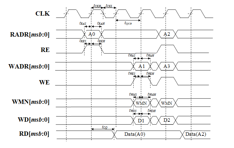
Fig. 80 Pseudo Dual Port RAM Timing
The RAMPDP behaves like a dual port RAM, but is created by double clocking a single port RAM. It can perform a ‘single read’ (1R), a ‘single write’ (1W) or a ‘read followed by write’ (1R+1W) operation in any given clock cycle. A read operation is performed when the signal RE is active high (RE= ‘1’). The output data will be driven to the output port RD in the same cycle read commands are issued. A latch holds the read data when ‘RE’=0. A write operation is performed when WE is high (WE= ‘1’). The input data must be put on the input data bus WD at the same time with the write command. Note that if the read and write address match during a (1R+1W) operation, i.e. RE=WE=’1’, the read data will contain the previous contents of the RAM (read occurs before write).
Synthesis
Overview
This release contains reference synthesis setup for the NVDLA design with Design Compiler (Wireload Model/Topographical).
Directory structure
The release directory structure for synthesis is shown below:
<NVDLA_RELEASE>
   |--- syn
   |--- scripts
   |       |--- syn_launch.sh
   |       |--- default_config.sh
   |       |--- dc_run.tcl
   |       |--- dc_interactive.tcl
   |       `--- dc_app_vars.tcl
   |--- templates
   |       |--- config.sh
   |       `--- cg_latency_lut.tcl
   `--- cons
          |--- NV_NVDLA_partition_a.sdc
          |--- NV_NVDLA_partition_c.sdc
          |--- NV_NVDLA_partition_m.sdc
          |--- NV_NVDLA_partition_o.sdc
          `--- NV_NVDLA_partition_p.sdc
NV_NVDLA_partition_* are synthesis “TOP_NAMES” - The designs will be compiled at this
hierarchy, and netlists will be generated for these designs. These are independent
sub-designs for synthesis, which are instantiated in a top-level wrapper.
Requirements
You will need a *NIX machine able to run Design Compiler. The scripts have been tested with Design Compiler version 2016.12 and newer. Memory and CPU requirements vary.
Synthesis Configuration
To be able to run synthesis, you will need a config file - You can use the “<NVDLA_ROOT>/syn/dc/templates/config.sh” file as reference. This file is in “bash” syntax.
There are many required and optional variables. Table below lists the supported variables, meanings and defaults.
Variable |
Comments |
|---|---|
|
Location on disk for the NVDLA source “hw” directory. |
|
Space separated list of TOP_NAMES to synthesize. You may choose to synthesize all or a subset of TOP_NAMES. Defaults to “NV_NVDLA_partition_a NV_NVDLA_partition_c NV_NVDLA_partition_o NV_NVDLA_partition_m NV_NVDLA_partition_p” |
|
Space separated list of search paths (directories) for locating all the pieces of RTL.
Defaults to an empty string.
Please do not include paths to non synthesizable (behavioral) RAM models, like the ones in |
|
Space separated list of search paths (directories) for locating all the supplementary Verilog include files. Defaults to an empty string. |
|
List of files to read in, apart from the modules that can be found in the search paths. Defaults to an empty string. |
|
List of extensions for the source RTL files. Defaults to “.v .sv .gv” |
|
List of extensions for supplementary Verilog include files. Defaults to “.vh .svh” |
|
Path to directory containing floorplans in the “DEF” format. Files should be named by the TOP_NAMES, with the extension “.def” This variable defaults to a directory called “def” in the current directory We do not provide templates, because it depends on the process node, and the memory compiler being used. |
|
Path to directory containing constraints in the “SDC” format. Files should be named by the TOP_NAMES, with the extension “.sdc” This directory may also contain “<TOP_NAME>.tcl” to specify any non-SDC constraints to guide synthesis. All of these constraints are sourced before compiling the design. This variable defaults to a directory called “cons” in the current directory. We provide template SDCs for all logical partitions in the ${NVDLA_ROOT}/syn/cons directory including clock constraints etc. You may provide your own constraints, based on the process node you are targeting. |
Variable |
Comments |
|---|---|
|
Location of the Design Compiler installation. Defaults to an empty string |
Variable |
Comments |
|---|---|
|
Path to a single standard cell library that will be used to map the design to (the “target” library). Defaults to an empty string. |
|
Path to all the libraries that are required to link the design. This should include the target library as well. Include any RAM compiler timing libraries here. Defaults to an empty string. |
|
Path to the “Milkyway Technology File” that is used to create the Milkyway models for the physical library. Please check with your standard cell library vendor for the right file to use. Defaults to an empty string. Required for DC-Topographical |
|
Path to the “TLUPlus” files that will be used for RC extraction Please check with your standard cell library vendor for the right file to use. Defaults to an empty string. Required for DC-Topographical |
|
Path to the “Tech2ITF” mapping file, that maps layer names from between the Milkyway Tech file and the interconnect technology format file. Please check with your standard cell library vendor for the right file to use. Defaults to an empty string. Required for DC-Topographical |
|
Bottom routing layer for signal nets. Please check with place-and-route methodology for the right value. Defaults to an empty string. Required for DC-Topographical |
|
Top routing layer for signal nets. Please check with place-and-route methodology for the right value. Defaults to an empty string. Required for DC-Topographical |
|
Space separated list of layers with preferred horizontal routing. Defaults to an empty string. |
|
Space separated list of layers with preferred vertical routing. Defaults to an empty string. |
|
Space separated list of regular expressions for cells that you do not wish to map your design to. A “dont_use” will be applied on these cells in Design Compiler. Defaults to an empty string. |
|
A file containing a “wireload model” - a lookup table for resistance and capacitance calculation based on fanout. Refer to the lcug16_Defining_Wire_Load_Groups.htm on the Synopsys Solvnet site for more information regarding wire load modeling. Not required if your standard cell library contains the wireload models built in. Not required for DC-Topographical. Defaults to an empty string. |
|
Name of the wireload model lookup table (if you have multiple tables) Not required for DC-Topographical. Defaults to an empty string. |
Warning
We do not supply timing models or synthesizable RTL for the RAMs in the design. These need to be provided by the user for the process node/ memory compiler being used.
Please DO NOT include ${NVDLA_ROOT}/vmod/rams/model in the RTL_SEARCH_PATH - They are simulation models, not synthesizable.
Variable |
Comments |
|---|---|
|
Boolean, “1” to enable over constraining the CG-Enable paths. See section 5.5.2 below Default is set to “0” |
|
File containing the fanout-based CG over constraint lookup table to pessimize the CG enable paths. See section 5.5.2 below. Please see “${NVDLA_ROOT}/syn/templates/cg_latency_lut.tcl” for an example. Defaults to an empty string. |
|
The number of CPU cores available for Design Compiler. Defaults to ‘1’ Note: Single CPU core synthesis may see a long overall runtime. |
|
Boolean, “1” to Run quick area optimization by undoing some optimizations on paths with positive slack. Defaults to “1”. |
|
Number of rounds of incremental compiles to run in Design Compiler. Defaults to “1” - This amounts to 2 rounds of compile, one for mapping - the “main” compile and one for incremental optimization - the “incremental” compile. |
|
String. Defaults to an empty string. This will be pre-fixed to the dc_shell command . Use this to manage job submission on LSF farm or grid, as appropriate. Use literal strings “<MODULE>” and “<LOG>” to substitute module name and log directory for each TOP_NAMES. In the absence of a command prefix, the synthesis jobs for each TOP_NAMES will run serially. If you do provide a command prefix, make sure that it is non-blocking, so that all synthesis jobs can be parallelized. Otherwise, the jobs are run serially. Example: export COMMAND_PREFIX="bsub -q some_queue -o <LOG>/<MODULE>.lsf.log"
|
Synthesis constraints
Clock Constraints
The clock constraints are provided through an SDC file. You will find reference constraints in “${NVDLA_ROOT}/syn/cons/NV_NVDLA_partition*.sdc”. These contain clock targets for the 16nm process. You will need to scale the clock constraints to the target process/synthesis corner as appropriate. The SDC files also contain some timing exceptions (false paths) as well. Please populate the SDC files for all TOP_NAMES in a single directory, and set the CONS variable in the configuration file described in the previous section.
You can also add additional non-SDC constraints, like, for example, specific clock gating styles, etc. in <CONS>/NV_NVDLA_partition*.tcl
Clock Gate Enable Path Over constraining
The flow allows for over constraining the CG enable paths to pessimize synthesis to take into account post-CTS latencies. This is achieved through a fanout-based lookup table in TCL syntax. See “${NVDLA_ROOT}/syn/templates/cg_latency_lut.tcl” for an example. Provide the path to this file as the CGLUT_FILE variable in the configuration file. To enable the over constraining, please set TIGHTEN_CGE variable to 1 in the configuration file.
Physical Constraints
If you are running physical synthesis, you can provide floorplans in DEF syntax for RAM/IO placement as input, depending on your physical implementation. Populate the DEF files for all TOP_NAMES in a single directory, and provide the path to the directory as the DEF variable.
You can also provide constraints in TCL syntax, through “<CONS>/NV_NVDLA_partition*.tcl” files.
Running synthesis
You can run synthesis using the “${NVDLA_ROOT}/syn/dc/scripts/syn_launch.sh” bash script. The supported arguments to the scripts are in table below.
Argument |
Explanation |
|---|---|
|
Path to the synthesis configuration file (see section 5.4) If not provided, the flow will look for a file called “config.sh” in the current directory. |
|
Specifies which tool to use for synthesis. Use one of the following: “wlm” => Use Design Compiler (non-topographical) for wireload model based synthesis (non-physical)
“dct” => Use DC-Topographical
“dcg” => Use DC-Graphical along with “-spg” in the compile command.
“de” => Use DC Explorer for synthesis.
|
|
Sandbox of synthesis. Optional.
Defaults to “ |
|
Space separated list of modules to run synthesis on / restore database for. If not specified, the TOP_NAMES must be populated in the configuration file. |
|
Path to design database (in DDC format) to restore. |
Running Non-physical synthesis (Wireload Models)
You can run:
${NVDLA_ROOT}/syn/dc/scripts/syn_launch.sh -mode wlm -config /path/to/config.sh
You will need to have a wire load model defined in your standard cell library, or in a separate file (in liberty syntax, as described in the lcug16_Defining_Wire_Load_Groups.htm on Synopsys solvnet)
In the configuration file the following variables are required to be defined:
WIRELOAD_MODEL_NAME
TARGET_LIB
LINK_LIB
DC_PATH
The following variables are optional:
WIRELOAD_MODEL_FILE
Running physical synthesis
You can run one of the following, To pick DC-Topographical/DC-Graphical/DC Explorer:
${NVDLA_ROOT}/syn/dc/scripts/syn_launch.sh -mode dct -config /path/to/config.sh
${NVDLA_ROOT}/syn/dc/scripts/syn_launch.sh -mode dcg -config /path/to/config.sh
${NVDLA_ROOT}/syn/dc/scripts/syn_launch.sh -mode de -config /path/to/config.sh
In the configuration file, the following variables are required to be defined:
TARGET_LIB
LINK_LIB
MW_LIB
DC_PATH
TF_FILE
TLUPLUS_FILE
TLUPLUS_MAPPING_FILE
MIN_ROUTING_LAYER
MAX_ROUTING_LAYER
Additionally, you may require the following variables depending on how your physical library views were built:
HORIZONTAL_LAYERS
VERTICAL_LAYERS
Restoring a design database
You can run one of the following, To restore a design database from a previous synthesis run with the reference methodology:
${NVDLA_ROOT}/syn/dc/scripts/syn_launch.sh -mode <mode_used_for_synthesis> -config /path/to/config.sh -build <build_tag_used_for_synthesis> -restore /path/to/build/db/<module>.ddc -modules <module>
Synthesis outputs
In the synthesis sandbox, the following outputs are generated:
<BUILD>
   |--- fv
   |     `--- NV_NVDLA_parition*
   |              `--- NV_NVDLA_parition*.svf
   |--- net
   |     |--- NV_NVDLA_partition*.gv (Mapped Netlist)
   |     |--- NV_NVDLA_partition*.full.def (complete output DEF)
   |     `--- NV_NVDLA_partition*.sdc (Output SDC)
   |--- db
   |     `--- NV_NVDLA_partition*.ddc (Synthesis design Database)
   |           (There are also a few intermediate design databases here)
   `--- report
           |--- NV_NVDLA_partition*.check_design
           |--- NV_NVDLA_partition*.check_timing
           `--- NV_NVDLA_partition*.final.report
                      (Detailed timing/QoR information)
                      (There are also reports generated at intermediate stages)
Here is the end of Integrator’s Manual.